China Semiconductor CMP Pad and Slurry 2026 — From DuPont Monopoly to Dual Domestic Substitution by Dinglong and Anji
Industry Research Institute | 2026-06-20
Chapter 1 Industry Overview and CMP Definition
1.1 Chemical Mechanical Planarization: The Indispensable Bridge Between Deposition and Lithography
Among the hundreds of process steps in semiconductor chip manufacturing, chemical mechanical planarization (CMP) stands as the irreplaceable global planarization step connecting thin-film deposition and photolithographic patterning. Its essence lies in the precisely coordinated application of chemical corrosion and mechanical abrasion to the wafer surface, abrading local protrusions down to sub-nanometer-level flatness at the nanometer and sub-angstrom scale, thereby providing the extreme planar substrate demanded by the depth-of-focus (DoF) requirements of subsequent lithography.
Without CMP, the multi-level metal interconnect structures of advanced-node integrated circuits — copper or aluminum interconnects, tungsten plugs, through-silicon vias (TSVs), and so forth — would accumulate hundreds to thousands of nanometers of surface topography at each deposited layer, preventing lithographic focus from landing on a planar reference plane and causing runaway linewidth variation and yield collapse. CMP is therefore not an optional auxiliary step but one of the physical prerequisites for advanced-node mass production.
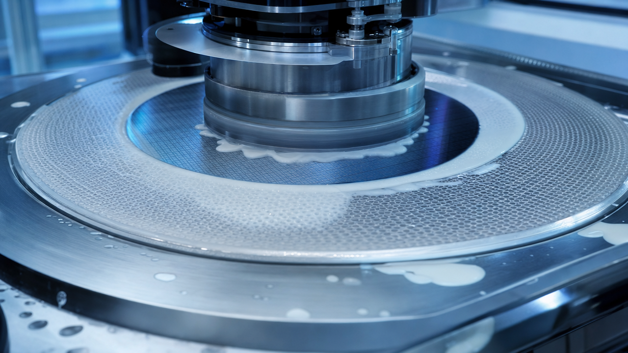
The basic mechanics of CMP: The wafer, face down, is clamped in a carrier head and pressed, at several tens of revolutions per minute, against the surface of a similarly rotating polyurethane polishing pad. A multi-component slurry — formulated from nano-abrasive particles, an oxidizer, a corrosion inhibitor, a chelating agent, pH adjusters, and surfactants — is delivered continuously through a supply line to the center of the pad, forming a thin fluid layer at the wafer-pad interface. Under the combined effect of downforce, linear velocity, and chemical action, protrusions on the wafer surface experience more intense interaction with abrasive particles and chemicals and are preferentially removed, while recesses are relatively protected by the fluid cushion, achieving global planarization. At the micro-scale, the mechanism couples nano-scale mechanical friction between abrasive particles and the wafer surface with chemical oxidation / dissolution / passivation — neither alone is sufficient.
Why multiple CMP steps are required: Modern advanced ICs traverse as many as 20–35 CMP steps from substrate to top metal layer, spanning shallow trench isolation (STI) oxide planarization, polysilicon gate planarization, tungsten plug (W plug) planarization, copper dual-damascene CMP (bulk copper removal + barrier removal), and inter-level dielectric (ILD) planarization among others. Each CMP step corresponds to one or more specialty semiconductor polishing materials (pad and slurry). As a result, CMP consumable consumption scales directly with process sophistication — the more advanced the node, the more CMP steps, and the greater the consumable demand.
1.2 The Strategic Weight of CMP Consumables in Semiconductor Materials
Semiconductor materials form the material foundation of chip manufacturing, spanning seven core categories: silicon wafers, photoresists, electronic specialty gases, wet electronic chemicals, photomasks, sputtering targets, and CMP consumables. In the global semiconductor materials market (approximately USD 75 billion in 2024), CMP consumables account for roughly 7%–8%, or about USD 46–55 billion.
That share may appear modest, but the strategic importance of CMP consumables far exceeds what market share alone implies, for three reasons:
First, high consumption frequency. Polishing pads are single-use consumables with service lives of only about 500–1,000 hours (roughly 1,000–2,000 wafers), meaning a single 12-inch production line may consume thousands of pads per month. Slurry is likewise used once and discarded — waste slurry containing abrasive particles, metal ions, and organic solvents constitutes hazardous waste that cannot be recovered. High-frequency consumption means CMP consumables are a continuous, incompressible component of wafer-fab operating costs.
Second, tight process coupling. CMP materials — especially slurry formulations — are intimately coupled to the specific process window of each downstream wafer fab (tool model, process temperature, downforce settings, target layer material). Switching suppliers requires a full process requalification lasting approximately 18–36 months, creating extreme switching costs and strong customer lock-in.
Third, essential domestic substitution imperative. Against the backdrop of escalating US–China technology competition and steadily expanding export controls, CMP materials have been designated a priority domesticization target in China's semiconductor industry policy. Both the National IC Investment Fund's directed investments and wafer-fab procurement policies' "domestic content KPI" are accelerating domestic substitution at an unprecedented pace.
1.3 The CMP Consumable Product Tree
CMP semiconductor consumables divide into five major sub-categories:
(I) CMP Pads
The polishing pad is the direct abrasive medium in CMP, made primarily from polyurethane. By structure and hardness:
- Hard polyurethane foam pads (Hard Pads): such as DuPont IC1000/IC1010, Shore D hardness 50–65, with precision micropore structure (pore diameter 20–100 µm), used for planarizing metal layers (tungsten, copper) and oxides (ILD). The workhorse product for advanced-node CMP.
- Soft stack pads (Soft Stack Pad / Politex): typically a hard top pad laminated with a soft foam sub-pad; the soft sub-pad absorbs pressure non-uniformities from wafer topography. Used for final metallization layers where scratch sensitivity is paramount.
- Fixed abrasive pads (FA Pads): abrasive particles are embedded directly in the pad body, reducing dependence on slurry-borne abrasives; used in specific applications such as sapphire substrate polishing.
(II) CMP Slurry
CMP slurry is a precision chemical system composed of nano-abrasives, chemical additives, and ultra-pure water. By application:
- Copper CMP slurry (Cu Slurry): bulk copper removal (Step 1) and barrier layer (Ta/TaN) removal (Step 2/3) in dual-damascene copper interconnects — the highest-volume slurry category at sub-20nm nodes.
- Tungsten CMP slurry (W Slurry): for W plug planarization; abrasive is typically alumina, oxidizer is ferric ion (Fe³⁺) or H₂O₂.
- STI / oxide slurry: for shallow trench isolation; abrasive is typically colloidal ceria (CeO₂), with stringent SiO₂/Si₃N₄ selectivity requirements.
- SiC specialty slurry: for pre-epitaxy and post-epitaxy SiC wafer polishing; SiC's ultra-high hardness (Mohs 9.5) demands specialized formulations.
- Advanced packaging CMP slurry: for TSV copper CMP, RDL copper CMP, and hybrid bonding ultra-planarization; extreme WIWNU and defect-density requirements.
(III) Post-CMP Cleaning Chemicals
After each CMP step, nano-abrasive particles (10–100 nm), organic residues, and metal ions (Cu²⁺, Fe³⁺, Ce³⁺, etc.) remain on the wafer surface. These must be removed to prevent contact-resistance increase, leakage current, yield loss, and device failure. Post-CMP cleaners divide into alkaline (ammonia-based, amino-acid chelate) and acidic (dilute HF) formulations, used with PVA brush scrubbing or megasonic cleaning to achieve >99.9% particle removal. Key suppliers include Entegris (wet chemicals), Gelinde (China), and Jianghuawei (China).
(IV) CMP Conditioners (Pad Dressers)
Pad conditioners (diamond pad conditioners) maintain the working surface of CMP pads. As pads accumulate abrasive particles and polishing residues, their micropore structures become clogged ("pad glazing"), causing material removal rates (MRR) to plummet. Diamond conditioners restore pad surface texture and porosity through directed micro-cutting (in-situ or ex-situ), maintaining consistent polishing performance.
The core technology lies in CVD diamond coating and precision fixation of diamond particles on a stainless-steel substrate (brazed or electroplated). The global market is dominated by 3M (USA), Entegris/Saesol (Korea), and Kinik (Taiwan). Domestic mainland China alternatives are virtually non-existent — import dependence approaches 100%, making this the weakest link in CMP supply-chain localization.
(V) CMP Equipment
CMP equipment (CMP tools / polishers) are the capital equipment executing the CMP process. The global market is dominated by Applied Materials (Reflexion GT series) and Ebara (F-REX series). China's domestic leader is Hwatsing Technology (688120, Uni-CMP series), which captured over 31% domestic market share in 12-inch CMP equipment by 2022.
Chapter 2 Global Landscape and China's Position
2.1 The Global CMP Materials Oligopoly
The global CMP pad market is dominated by DuPont (formerly Rohm and Haas Electronic Materials, acquired 2009), which holds approximately 75–80% global CMP hard pad share via its IC1000/IC1010 product family. The 2024 global CMP pad market is estimated at USD 1.8–2.2 billion. Secondary players include JSR (Japan, soft stacked pads), Cabot Microelectronics / CMC Materials (now part of Entegris), and 3M.
The global CMP slurry market (estimated USD 2.0–2.4 billion in 2024) is more fragmented. Key players by segment:
- STI/oxide slurry: Entegris (CMC Materials), DuPont, Fujimi (Japan)
- Copper CMP slurry: Entegris (CMC Materials), Fujifilm (Japan, ~20–30% of advanced Cu CMP), Anji Microelectronics (China, global #2 in certain Cu CMP segments)
- Tungsten CMP slurry: Entegris (CMC Materials), Cabot
- SiC slurry: Resonac (Showa Denko), Fujimi, Entegris, and emerging domestic Chinese suppliers
The 2022 acquisition of CMC Materials by Entegris for approximately USD 6.5 billion consolidated the #1 and #2 global CMP slurry suppliers, creating a combined entity with roughly 35–40% global CMP slurry share and an even stronger position in the highest-margin segments (advanced copper CMP, post-CMP cleaning).
2.2 China's Market Share — From Near-Zero to 15–25%
A decade ago, China's domestic CMP materials market was entirely import-dependent. Since 2016, a combination of policy tailwinds, R&D investment, and wafer-fab partnerships has driven domestic substitution to levels that are now visible in revenue data:
- CMP hard pads: Dinglong Co. (300054.SZ) is China's only manufacturer of 12-inch qualified hard polyurethane CMP pads in mass production. Domestic market share of CMP pads in China: estimated 15–25% (2025), primarily serving 12-inch wafer fabs (YMTC, CXMT, SMIC) in mature nodes.
- CMP slurry: Anji Microelectronics (688019.SH) is China's undisputed CMP slurry leader. Domestic market share in China approximately 15–20% (2025); global share approximately 8–11% (2025 estimate). Core strengths: copper CMP slurry and dielectric (STI/ILD) CMP slurry for mature nodes (≥28nm).
- Post-CMP cleaning: Gelinde (格林达), Shanghai Xinyang (上海新阳), and others serve the domestic cleaning chemicals market with meaningful domestic share in mature-node applications.
2.3 China's CMP Market Size — From USD 0.8B to USD 1.5B
The Chinese CMP materials market (all consumables combined) is estimated at approximately RMB 8–12 billion (USD 1.1–1.7 billion) in 2025, driven by rapid wafer capacity expansion:
- YMTC (long-term 3D NAND target: 300,000+ 12-inch wfpm)
- CXMT (DRAM, expanding to 150,000+ 12-inch wfpm)
- SMIC (mature foundry, multi-technology)
- Huahong Group (power IC, RF, mature processes)
As the world's largest single expansion region for wafer capacity (2023–2026), China accounts for a disproportionate share of global CMP consumable demand growth — estimated at 25–35% of incremental global demand through 2027.
Chapter 3 Core Technology
3.1 Polyurethane Foam Pad Engineering
The IC1000-type hard polyurethane pad — invented by Rodel (later acquired by Rohm and Haas, now DuPont) — has dominated CMP for over 30 years due to its unique combination of micro-porosity, mechanical rigidity, and chemical inertness. Its manufacture involves:
- Prepolymer synthesis: Toluene diisocyanate (TDI) or methylene diphenyl diisocyanate (MDI) reacts with polyols (polytetramethylene ether glycol, PTMEG, or polypropylene glycol) to produce an isocyanate-terminated polyurethane prepolymer.
- Curing / foam formation: A curative (typically 4,4'-methylene-bis(2-chloroaniline), MBCA) is mixed with hollow microspheres (glass or polymer, 40–100 µm diameter) into the prepolymer and cast in molds. During curing, the microspheres create the characteristic micropore network that holds slurry and provides surface texture.
- Slicing and grooving: Cured polyurethane billets are sliced to target thickness (~1.5–3.0 mm for IC1000), then precision-grooved (concentric rings, radial grooves, or X-Y grid patterns) to control slurry distribution across the pad surface and facilitate spent slurry discharge.
Dinglong's manufacturing breakthrough: Replicating DuPont's IC1000 process requires mastering exact TDI/MDI prepolymer viscosity–temperature relationships, microsphere size distribution (D90 < 150 µm, CV < 15%), curing temperature curve control (±0.5°C precision), and multi-axis CNC grooving. Dinglong (300054.SZ) achieved the first domestic 12-inch qualified IC1000-equivalent hard pad around 2020–2021 after a decade of R&D, validating that this technology barrier — though formidable — is not insurmountable for a well-capitalized domestic manufacturer with polyurethane chemistry expertise.
3.2 Nano-Abrasive Chemistry: CeO₂, SiO₂, Al₂O₃
The three primary abrasive families in CMP slurry each have distinct chemical roles:
Colloidal ceria (CeO₂): The abrasive of choice for STI oxide CMP. Unlike fumed silica, CeO₂ achieves extremely high SiO₂ removal rates at low mechanical stress through a chemical "tooth" mechanism — Ce³⁺/Ce⁴⁺ redox cycling at the particle surface catalyzes Si–O bond breakage, enabling SiO₂/Si₃N₄ selectivity ratios of 100:1 or more. China has a strategic advantage in CeO₂ supply, as it commands approximately 38% of global rare-earth reserves and has developed full-spectrum rare-earth processing infrastructure.
Fumed silica (SiO₂): The dominant abrasive in copper CMP and ILD CMP slurries. Produced by flame hydrolysis of SiCl₄, fumed silica nano-particles (primary particle size 5–50 nm, BET surface area 50–380 m²/g) form a three-dimensional aggregate network in colloidal suspension. Semiconductor-grade fumed silica (metallic ion impurities ≤10 ppb) is dominated by Evonik (AEROSIL®), Cabot (CAB-O-SIL®), and OCI. Domestic Chinese producers have not yet achieved semiconductor-grade purity — a critical upstream vulnerability.
Alumina (Al₂O₃): The abrasive of choice for tungsten CMP and tungsten polishing slurries, due to alumina's higher hardness (Mohs 9 vs. silica's Mohs 7) enabling the aggressive mechanical removal of tungsten metal. Alumina abrasives present a greater risk of scratch defects (DLE, deep lateral erosion) if particle size distribution is poorly controlled; this requires narrow PSD (D99 < 200 nm) and rigorous large-particle count (LPC) management.
3.3 Cu vs. W vs. STI Formulation Differences
The three major CMP slurry families have fundamentally different chemical systems:
| Parameter | Cu CMP Slurry | W CMP Slurry | STI/Oxide Slurry |
|---|---|---|---|
| Abrasive | Fumed SiO₂ | Al₂O₃ | Colloidal CeO₂ |
| Oxidizer | H₂O₂ | H₂O₂ or Fe³⁺ | None (oxide is already oxidized) |
| Key additive | BTA (copper corrosion inhibitor) | — | Selectivity additive (Si₃N₄ suppressor) |
| pH | 2–4 (acidic) | 2–3 (acidic) | 5–8 (near-neutral to mildly acidic) |
| Target MRR | Cu: 300–1000 nm/min | W: 200–600 nm/min | SiO₂: 200–500 nm/min |
| Key challenge | Dishing, erosion, Low-k damage | Scratch defects, micro-loading | High selectivity vs. Si₃N₄ stop layer |
Chapter 4 Industry Supply Chain
4.1 Upstream Materials
The CMP consumable supply chain extends to several layers of upstream raw materials:
For CMP pads:
- TDI/MDI polyurethane prepolymers (from Covestro, Wanhua Chemical, Huntsman)
- Hollow microspheres for pore formation (from 3M Zeeospheres, Asia Pacific Microsphere)
- Specialty curing agents (MBCA, DMTDA) — primarily from Lanxess, Albemarle
For CMP slurry:
- Semiconductor-grade fumed silica (Evonik, Cabot, OCI — China has no qualified domestic supplier)
- High-purity colloidal ceria (China has full supply chain: Grirem, China Rare Earth Group)
- H₂O₂ (ultra-high purity, UHP grade, from Mitsubishi Gas Chemical, Solvay, and domestic producers)
- BTA (benzotriazole), EDTA, chelating agents (domestic specialty chemical producers in China)
- Ultra-pure water (UPW, 18.2 MΩ·cm) — fab-integrated, not separately supplied
4.2 CMP Endpoint Detection — The Process Integration Layer
CMP endpoint detection (EPD) technologies determine when to stop polishing and represent a critical integration point between the pad, slurry, and equipment:
- Motor Current Monitoring (MCM): the rotating carrier head's motor current changes when the polished layer changes from softer copper to harder dielectric — a simple but widely deployed in-situ endpoint signal.
- Optical Endpoint Detection (OED): a laser beam passes through a transparent window in the pad, reflects off the wafer surface, and is analyzed by a spectrometer. When the polished layer transitions (e.g., from copper to Ta barrier), the reflectance spectrum changes detectably.
- In-situ eddy current sensing: used specifically for copper CMP; an eddy-current sensor mounted below the pad platen detects changes in copper film thickness in real time, enabling closed-loop MRR control.
4.3 Diamond Pad Conditioner Technology
The key technical parameters of diamond pad conditioners are:
- Diamond particle size: typically 30–100 µm median diameter for standard IC production conditioners; smaller particles (15–40 µm) for advanced-node conditioners (to minimize scratch risk)
- Diamond fixation method: electroplated (lower cost, shorter life), brazed (stronger bond, longer life), or CVD-grown (highest uniformity, highest cost)
- Conditioner flatness: ≤5 µm flatness of the conditioning disk face; exceeding this tolerance causes non-uniform pad surface conditioning and WIWNU degradation
- Diamond layer uniformity: coefficient of variation (CV) of diamond particle height on the disk surface must be <10% to ensure uniform micro-cutting depth across the pad
Chapter 5 Downstream Applications
5.1 12-Inch Logic and Memory Wafer Fabs — The Core Demand Driver
The dominant demand source for CMP consumables is 12-inch (300 mm) wafer production for advanced logic and memory:
- 3D NAND (YMTC, Samsung, Micron): high layer counts (128L, 200L, 232L, 300L+) multiply CMP step counts. Each generation transition adds 2–4 CMP steps per wafer. YMTC's 232L NAND requires approximately 28–32 CMP steps per wafer.
- DRAM (CXMT, Samsung, SK Hynix): standard DDR5 DRAM requires approximately 15–20 CMP steps; HBM stacks require additional high-uniformity CMP for through-silicon via formation.
- Advanced logic (TSMC N3/N2, Samsung GAA): Gate-All-Around (GAA) transistor architectures introduce new nanosheet channel CMP requirements not present in FinFET structures.
5.2 8-Inch Wafer and Mature-Node Applications
Mature-node 8-inch wafer production (MEMS, power ICs, RF, analog, OLED driver ICs) represents a stable, price-sensitive CMP market. Key characteristics:
- Lower per-wafer CMP step count (8–12 steps typical)
- Greater price sensitivity — domestic CMP materials have highest penetration here
- Domestic suppliers (Anji, Dinglong, Gelinde) already hold >30% domestic market share in this segment
5.3 SiC Polishing — The Fastest-Growing Sub-Segment
Silicon carbide polishing for power semiconductor wafer production is the highest-growth CMP sub-segment (estimated CAGR 20–25% through 2030), driven by China's EV and solar power markets:
SiC's extreme hardness (Mohs 9.5) requires:
- Pre-epitaxy substrate CMP: using strong oxidizer slurries (KMnO₄, H₂O₂/catalyst systems) to achieve Ra <0.2 nm on 4H-SiC (0001) face
- Post-epitaxy surface preparation: even lower Ra (<0.1 nm) required before device fabrication
- CMP removal rates for SiC are inherently low (typically 20–100 nm/min vs. 300–1000 nm/min for copper), making process efficiency a key challenge
China's SiC substrate makers (TanKeBlue, SICC, Sictory) are rapidly scaling to serve domestic SiC power device fabs (BYD Semiconductor, CRRC, Silan Microelectronics), creating a fast-growing demand base for specialty SiC CMP slurry.
5.4 Advanced Packaging CMP
Advanced packaging — including CoWoS (Chip-on-Wafer-on-Substrate), SoIC (System-on-Integrated-Chips), and Hybrid Bonding — imposes some of the most stringent CMP specifications in the industry:
- Hybrid Bonding ultra-planarization: bonding surfaces must achieve WIWNU <0.3 nm (3-sigma) and zero detectable surface particles >20 nm — requirements that exceed even the most demanding front-end-of-line (FEOL) CMP specs
- TSV Cu CMP: must achieve near-zero dishing (<5 nm) and erosion (<10 nm) across TSV arrays of varying pitch and diameter
- RDL (redistribution layer) Cu CMP: requirement for ultra-low-defect copper redistribution layer, critical for fine-pitch flip-chip connections
Chapter 6 Key Players
6.1 DuPont — The Global Pad Monopolist
DuPont Electronic Materials (formerly Rohm and Haas Electronic Materials, acquired 2009) dominates the global hard CMP pad market with approximately 75–80% share. Key products: IC1000 (standard hard pad), IC1010 (lower porosity, higher hardness), Politex (soft stack pad). DuPont's CMP pad revenue is estimated at USD 1.3–1.7 billion annually (2024). Core manufacturing in the US (Newark, DE), with China localization via the Suzhou manufacturing base.
DuPont's competitive moat: 30+ years of formulation data and process correlation with virtually every wafer fab's CMP equipment and process recipe; the switching cost for fabs is extremely high.
6.2 Entegris (CMC Materials) — The Slurry Giant
Following the USD 6.5 billion acquisition of CMC Materials in 2022, Entegris became the world's largest CMP slurry supplier by revenue (estimated USD 800M–1.0B CMP slurry revenue, 2024). Core products: copper CMP slurry (SEMI-SPERSE, SEMI-W2000 series), tungsten CMP slurry (W7000 series), post-CMP cleaning (ATMI legacy products). Entegris also supplies the diamond pad conditioner (from the Saesol acquisition).
6.3 Dinglong Co. (300054.SZ) — China's CMP Pad Champion
Dinglong Co., founded 1999 in Wuhan as a printing consumables (toner) manufacturer, pivoted to semiconductor materials around 2014–2015 and achieved China's first domestic 12-inch CMP hard pad in mass production. Key milestones:
- 2018: first domestic 8-inch CMP pad in customer qualification
- 2020–2021: 12-inch CMP hard pad (IC1000-equivalent) achieves production qualification at YMTC, CXMT, SMIC
- 2023–2025: revenue from CMP pads exceeds RMB 400M, growing 60%+ YoY; expanding production capacity (Wuhan base Phase II, total capacity targeting 3M+ pads/year by 2027)
- 2025–2026: entering advanced-node evaluation (14nm and below); advancing into soft stack pad development
6.4 Anji Microelectronics (688019.SH) — China's CMP Slurry Leader
Anji Microelectronics, founded in 2000 in Shanghai by Andrew Teng (a returnee chemist with prior experience in the US and Taiwan semiconductor materials sector), has grown to become China's only significant CMP slurry company with qualified mass production at 12-inch advanced-node fabs. Key facts:
- Revenue ~RMB 900M–1.1B (2024 estimate), CAGR ~30% (2019–2024)
- Core products: copper CMP slurry (28nm qualified at SMIC, YMTC), STI/dielectric CMP slurry, barrier CMP slurry
- Global CMP slurry share: estimated 8–11% (2025), #4–5 globally
- R&D investment: ~15–18% of revenue annually; 300+ active patents
- Recent development: SiC CMP slurry entering qualification at domestic SiC wafer fabs
6.5 Other Domestic Players
- Hwatsing Technology (华海清科, 688120): CMP equipment (Uni-CMP series); domestic 12-inch CMP tool market share >40% (2025). Strategic partner to Dinglong and Anji in integrated solutions.
- Gelinde (格林达): post-CMP cleaning chemicals and copper polishing slurries; serves mature-node domestic wafer fabs.
- Shanghai Xinyang (上海新阳): semiconductor-grade chemicals including CMP post-clean chemicals; listed on Shanghai Stock Exchange.
- Jianghuawei (江化微): specialty wet chemicals for back-end processes including CMP cleaning; serves OSAT and mature foundry customers.
- Jinhe Electronics / Kinik (晶禾电子): diamond pad conditioners (Taiwan-based, domestic sales in mainland China); the only qualified conditioner supplier with significant domestic presence.
Chapter 7 Domestic Substitution Tier Map and Tianxia Gongchang Database Insights
7.1 Tier 1 (Mass Production, >20% Domestic Share): CMP Hard Pads and Cu/STI Slurry
Tier 1 — Fully qualified, in active mass production:
- 12-inch CMP hard pads at mature nodes (28nm–90nm): Dinglong, domestic share ~20–25%
- Copper CMP slurry (28nm+): Anji Microelectronics, domestic share ~15–20%
- STI/ILD CMP slurry (28nm+): Anji Microelectronics, domestic share ~12–18%
- Post-CMP cleaning chemicals (mature nodes): Gelinde, Shanghai Xinyang, combined domestic share ~25–35%
7.2 Tier 2 (Qualification Phase, Entering Production): Advanced-Node Slurry
Tier 2 — In customer process qualification at leading domestic fabs:
- Copper polishing slurry at 14nm and below: Anji Microelectronics in qualification at SMIC and YMTC advanced lines
- SiC CMP slurry: Anji, plus a handful of domestic startups, entering qualification at SICC, TanKeBlue
- 12-inch CMP soft stack pads: Dinglong in development; no mass-production domestic supplier yet
7.3 Tier 3 (R&D / Blank): Diamond Conditioners, Advanced-Node Slurry ≤7nm
Tier 3 — No domestic qualified supplier:
- Diamond pad conditioners: 0% domestic content for mainland China fabs (Kinik from Taiwan is used)
- Semiconductor-grade fumed silica (upstream raw material): 0% domestic production at required purity
- CMP slurry for GAA (2nm-equivalent) nodes: no domestic supplier in qualification
7.4 the platform Database Insights
the platform's database of 4.8 million active manufacturing enterprises in China provides unique supply-chain intelligence for the CMP materials sector. Keyword searches across the platform reveal:
- "Polishing pad": 39 manufacturers, concentrated in Jiangsu, Guangdong, and Hubei
- "Polishing liquid": 63 manufacturers, dominated by Shanghai and Jiangsu
- "Wet electronic chemicals": 44 manufacturers, a key proxy for CMP upstream chemical supply
- "Semiconductor consumables": 165 manufacturers, covering the full CMP supply-chain ecosystem
- "Advanced packaging": 21 manufacturers, indicative of demand-side customers for advanced CMP
This data reveals the geographic clustering of China's CMP materials ecosystem: East China (Shanghai, Jiangsu, Zhejiang) dominates high-purity chemical supply; Central China (Wuhan, Hubei) is the hub for CMP pad manufacturing; and Beijing-Tianjin is strong in rare-earth-derived CeO₂ abrasive supply.
Chapter 8 Pricing and Business Models
8.1 Global CMP Pad Pricing Structure
CMP pad pricing follows a tiered structure based on wafer size, application node, and certification level:
| Pad Type | Supplier | Price Range (USD/pad, 30-inch) | Notes |
|---|---|---|---|
| IC1000 (standard hard pad) | DuPont | USD 1,800–2,500 | Dominant product; >75% global market |
| IC1010 (high-hardness) | DuPont | USD 2,000–2,800 | Advanced-node premium |
| IC1000-equivalent | Dinglong | USD 140–180 | ~7–10% of DuPont price |
| Politex (soft stack) | DuPont | USD 900–1,400 | Final metal applications |
The dramatic pricing differential between DuPont and Dinglong (~90% discount) reflects:
- Dinglong's lower manufacturing cost (domestic labor, materials)
- Dinglong's penetration pricing strategy to displace incumbents
- Market acceptance of some performance trade-offs at mature nodes
8.2 CMP Slurry Pricing
CMP slurry pricing varies dramatically by application:
- Advanced Cu CMP slurry (≤7nm): USD 35–80/liter (imported, Entegris/Fujifilm)
- Standard Cu CMP slurry (28nm+): USD 15–35/liter (imported); RMB 20–35/liter (Anji domestic)
- STI/oxide slurry: USD 8–20/liter (imported); RMB 8–18/liter (Anji domestic)
- SiC CMP slurry: USD 40–100/liter (imported); RMB 25–60/liter (domestic, limited supply)
8.3 Business Model: From Spot Supply to Long-Term Agreements
Leading CMP materials companies employ two primary commercial models:
Long-term supply agreements (LTA): Multi-year volume commitments with quarterly price adjustments (linked to raw material indices). Dominant model for Tier-1 wafer fab customers (TSMC, Samsung, YMTC). Provides revenue predictability for suppliers; price adjustment caps protect against commodity inflation.
Consignment / just-in-time delivery: Customer-managed inventory held at CMP supplier's regional warehouse, with fab drawing on stock as needed. Reduces fab working capital and stock-out risk; enables faster emergency replenishment.
Domestic suppliers (Dinglong, Anji) are increasingly moving their major customers (YMTC, CXMT, SMIC) onto LTA structures as their product qualification status matures from "approved alternative" to "preferred supplier."
Chapter 9 Representative Customer Cases
9.1 YMTC and Dinglong: The Pioneer Domestic Pad Certification
Yangtze Memory Technologies (YMTC) is China's leading 3D NAND manufacturer and was among the first fabs to systematically pursue domestic CMP pad qualification as a supply security strategy. The YMTC–Dinglong relationship exemplifies the domestic substitution trajectory:
- 2018–2019: Dinglong submits first IC1000-equivalent 12-inch hard pad samples to YMTC engineering team for initial screening
- 2020: YMTC approves Dinglong pad for "extended evaluation" (limited production trial) on select mature-node CMP tools; initial split: 5–10% Dinglong / 90–95% DuPont
- 2021–2022: Following YMTC's addition to the US Entity List (October 2022), domestic content procurement pressure intensifies; Dinglong pad allocation rises to 25–40% of YMTC's hard pad consumption
- 2023–2025: Dinglong pad achieves "qualified supplier" status at YMTC for 128L NAND process nodes; allocation exceeds 40% on qualified tools; process window still narrower than DuPont IC1000 at leading nodes
- 2026 outlook: Dinglong targeting >50% allocation at YMTC mature lines; 232L node qualification in progress (expected completion H2 2026)
9.2 SMIC and Anji: Copper CMP Slurry at Advanced Nodes
SMIC (Semiconductor Manufacturing International Corp., 688981/0981.HK) and Anji Microelectronics have built one of China's deepest CMP slurry qualification partnerships:
Anji's copper CMP slurry is qualified at SMIC's N+1 (approximately 7nm-class) process node — a technical milestone demonstrating that domestic slurry can meet the formidable WIWNU (<1.5%) and LPC defect (<100 particles/mL at >50nm) specifications required at sub-10nm equivalent process nodes. This achievement, confirmed in Anji's 2024 annual report disclosures, positions Anji as the only domestic Chinese slurry company with sub-10nm node Cu CMP qualification at a major domestic fab.
Chapter 10 Investment and M&A
10.1 The CMC Materials / Entegris Consolidation (2022)
The USD 6.5 billion Entegris–CMC Materials merger (completed November 2022) was the largest transaction in CMP industry history. Strategic rationale:
- Combined entity achieves top-3 global position in CMP slurry, post-CMP cleaning, and pad conditioning
- Cross-selling opportunities: Entegris brings semiconductor-grade ultra-pure materials handling; CMC brings CMP process expertise
- Regulatory challenge: the DOJ required Entegris to divest CMC's pipeline control and microelectronics pipeline systems businesses, but CMP materials were cleared with no divestiture requirement
10.2 JSR's Private Equity Exit (2023)
JSR Corporation, one of Japan's leading semiconductor photoresist and CMP materials suppliers, was taken private in 2023 by JIC (Japan Investment Corporation), a state-backed PE fund, for approximately JPY 960 billion (USD 6.4 billion). This privatization was widely interpreted as the Japanese government seeking tighter strategic control over critical semiconductor material supply chains, with an implicit objective of ensuring JSR's advanced materials (ArF/EUV photoresist, CMP slurry) remain available to Japan-allied chip manufacturers while restricting supply to potential adversaries.
10.3 Domestic Chinese Investment in CMP Companies
- Dinglong Co. (300054): National IC Fund II invested in a private placement in 2022; major strategic shareholders include several Chinese insurance funds and domestic semiconductor sector ETFs
- Anji Microelectronics (688019): STAR Market IPO (July 2019) raised ~RMB 1.5B; subsequent secondary offerings to fund capacity expansion and R&D
- Hwatsing Technology (688120): received National IC Fund support; key strategic investor in CMP equipment domesticization
10.4 International M&A Targeting Chinese CMP
Unlike in photoresist or EUV optics, international CMP companies have not pursued aggressive acquisition of Chinese CMP firms — partly due to regulatory concerns on both sides, and partly because Chinese CMP firms are now large enough (Anji market cap ~RMB 30–40B) that acquisition would be strategically complex. Instead, technology licensing and distribution arrangements have been the preferred cross-border commercial structure.
Chapter 11 Policy and Standards
11.1 National Semiconductor Material Policy Framework
China's policy support for domestic CMP materials operates through multiple channels:
National IC Investment Fund (大基金): Fund I (USD 20B, 2014) focused primarily on wafer fab equipment; Fund II (USD 28B, 2019) expanded into materials; Fund III (RMB 344B / ~USD 47B, established May 2024) explicitly targets upstream materials and chemicals as a priority, with CMP consumables among the named focus areas.
First-Article / 首台套 Policy: Products listed in the "Key New Materials Application Demonstration Guidance Catalog" (including domestic CMP pads and slurry qualifying at leading domestic fabs) receive government-backed insurance compensation for wafer fabs that adopt them. This policy directly addresses the "chicken-and-egg" problem of domestic material adoption — wafer fabs are compensated if a newly qualified domestic material causes yield loss, dramatically reducing the risk of initial adoption.
"14th Five-Year Plan" for Integrated Circuits: Explicitly calls for achieving ≥40% domestic content in CMP materials by 2025, and ≥60% by 2030, for mature-node (≥28nm) processes at domestic wafer fabs.
11.2 Standards Framework
China is actively building a domestic CMP standards framework through:
- Participation in SEMI China committee working groups (translating and localizing SEMI M55, SEMI F57, and CMP-specific SEMI standards)
- Development of national standards for "Semiconductor CMP Slurry Technical Specifications" through the China Electronics Standardization Institute
- Anji Microelectronics and Dinglong are both active in relevant standards drafting committees
11.3 US Export Control: Impact on CMP Supply
US export controls (Entity List additions and EAR amendments since 2019) directly affect CMP materials supply to China:
- DuPont's advanced-node CMP pad supply to Entity List wafer fabs (YMTC, CXMT) has become legally complex, accelerating those fabs' domestic substitution urgency
- Entegris's China business (estimated ~20–25% of revenue) faces ongoing compliance evaluation; advanced-node slurry supply to restricted Chinese fabs has been curtailed
- These restrictions paradoxically accelerate domestic substitution — the very fabs most targeted by export controls have the strongest incentive to qualify domestic alternatives
Chapter 12 Trends and the Research Institute Research Institute Assessment
12.1 GAA Transistor Structures and New CMP Requirements
Gate-All-Around (GAA) transistor architectures, entering mass production at Samsung (3GAE, 2022) and TSMC (N2, 2025), introduce nanosheet channels that require new CMP process steps not needed in FinFET:
- Nanosheet release CMP: after the channel release etch, remaining SiGe sacrificial layers must be selectively removed; CMP steps here must achieve angstrom-level uniformity
- High-k dielectric CMP selectivity: HfO₂/HfSiO gate dielectric must be preserved with near-zero erosion while adjacent metal gate material is removed
- Extreme low-defect requirements: any CMP-induced scratch or particle defect on a GAA nanosheet causes catastrophic transistor failure — LPC requirements below 5 particles/mL at >20nm
12.2 The 2nm Era and Beyond
At TSMC N2 and Samsung 2GAP (both in/near production by 2025–2026), CMP is required at 30–35+ steps per wafer, with each step requiring progressively tighter WIWNU (<1.0%), lower defect density, and higher process repeatability. This raises the technical barrier for domestic CMP entrants:
- Dinglong's 12-inch hard pads are currently qualified to ~28nm equivalent; 14nm qualification expected by 2026; sub-5nm by 2030 remains uncertain
- Anji's Cu CMP slurry is qualified at SMIC N+1 (~7nm class); 3nm-equivalent qualification timeline is beyond 2027
12.3 SiC CMP — The Next Localization Frontier
With China's SiC polishing market expected to reach RMB 1.5–2.5B by 2028, SiC CMP slurry is the most visible near-term growth opportunity for domestic materials companies:
- Anji Microelectronics is the frontrunner for domestic SiC CMP slurry at 6-inch and 8-inch SiC wafer fabs
- SMIC-affiliated and independent SiC fab investments in China (BYD, Silan, CRRC) are the target customer base
- Technical hurdle: achieving Ra <0.1 nm on 4H-SiC with domestic slurry; currently 0.15–0.2 nm achievable; closing the gap by 2026–2027 is feasible
12.4 the Research Institute Research Institute Assessment
Combining industry data, company disclosures, and market intelligence, the Tianxia Gongchang Research Institute makes the following assessments for China's CMP materials sector through 2030:
Domestic CMP pad share will reach 35–45% of the China market by 2028: Dinglong is the near-certain winner in CMP hard pads; soft stack pads and fixed-abrasive pads represent Tier 2 opportunity for a domestic entrant by 2027–2028.
Anji Microelectronics will reach 20–25% China CMP slurry share by 2027: The path is clear for mature nodes; advanced-node (≤14nm) qualification at YMTC/CXMT is the key milestone that would unlock an additional 8–12 percentage points of share.
Diamond pad conditioners remain the supply chain's most critical vulnerability: With 0% domestic mainland production, any disruption to Kinik (Taiwan) or international conditioner supply would immediately halt CMP operations at all domestic wafer fabs. This is a strategic gap that deserves policy-level priority investment.
SiC CMP slurry is a USD 400–700M domestic market opportunity by 2030: First-mover domestic qualification in this segment (likely Anji or a well-funded startup by 2026) will lock in multi-year supply relationships with a rapidly scaling domestic SiC fab ecosystem.
The "dual vendor" strategy will become standard at all domestic Tier-1 fabs: Following YMTC's precedent, CXMT, SMIC, and Huahong will all target ≥50% domestic content in CMP pads and ≥30% in CMP slurry by 2027, driven by both supply security and policy compliance.
Chapter 13 Risks
13.1 Technology Maturation Risk at Advanced Nodes
The single greatest risk to domestic CMP companies' growth trajectories is technology maturation lag at leading-edge nodes. Specifically:
- DuPont's 3nm-era pad technology includes proprietary "nano-textured" pad surface treatments developed over 10+ years of collaboration with TSMC and Samsung — this institutional knowledge cannot be replicated quickly
- Entegris's advanced Cu CMP slurry for sub-5nm involves formulation optimizations that Anji has not yet achieved; the technical delta is measurable in defect density (
50 vs. ~20 particles/mL) and WIWNU (1.5% vs. ~0.8%) — gaps that become yield-critical at leading-edge nodes - Timeline risk: if TSMC/Samsung advanced-node IC production shifts more rapidly to sub-3nm than domestic Chinese fabs can follow, domestic CMP companies may never close the technology gap with the leading international players in the most advanced applications
13.2 Upstream Material Dependency
Domestic CMP companies remain dependent on imported upstream materials for their highest-performance products:
- Semiconductor-grade fumed silica: 100% import-dependent; any Evonik/Cabot export restriction would force formulation changes with unpredictable yield impact
- Specialty curative agents (MBCA) for polyurethane pads: largely imported from Lanxess/Albemarle; domestic alternatives under development but not yet at required purity
- Advanced-node H₂O₂ (UHP grade): domestic supply exists but quality consistency for sub-10nm applications requires further validation
13.3 Price Pressure from Oversupply
Mature-node wafer capacity oversupply (2023–2025) created downward price pressure on CMP consumables:
- Reported 10–20% price reductions in mature-node CMP slurry (2023–2024 vs. 2022 peak)
- If multiple domestic suppliers simultaneously reach qualification for the same slurry category (e.g., STI slurry at 28nm), intra-domestic price competition could compress gross margins further
- Dinglong's pad pricing, already at a deep discount to DuPont, has limited room for further reduction without impacting R&D investment capacity
13.4 Intellectual Property Risk
As domestic CMP companies begin targeting international customers (TSMC Taiwan, Samsung Korea), they will face rigorous IP compliance scrutiny:
- Freedom-to-operate (FTO) analysis against DuPont, Entegris, and JSR's active patent portfolios is a continuous requirement
- The risk of patent litigation (even if ultimately resolved through cross-licensing) could temporarily disrupt customer relationships and management bandwidth
- Anji's 300+ patent portfolio and Dinglong's 200+ CMP-related patents provide a meaningful defensive IP shield, but a coordinated assertion campaign from a deep-pocketed incumbent could be costly to defend
Chapter 14 Data Sources
Primary Data Sources and References
This report draws on the following sources, prioritizing data that is cross-verifiable and of high credibility:
Market Data:
- Mordor Intelligence, Chemical Mechanical Planarization (CMP) Market — Global Industry Analysis, Size, Share, Growth, Trends and Forecast 2024–2029, published 2024
- Markets and Markets, CMP Slurry Market by Type (STI, W, Cu, Dielectric)... Global Forecast to 2027, 2022 update
- Gartner, Semiconductor Manufacturing Materials Spending Tracker (2024–2026 quarterly data)
- IC Insights, Global Wafer Shipment and Capacity Report, 2025 edition
Company Filings and Public Disclosures:
- Anji Microelectronics (688019.SH) Annual Reports 2024–2025 (Shanghai Stock Exchange)
- Dinglong Co. (300054.SZ) Annual Reports 2024–2025 (Shenzhen Stock Exchange)
- DuPont de Nemours (DD) 2024 Annual Report, Electronics segment
- Entegris (ENTG) 2024–2025 Annual Reports, post-CMC Materials integration
- Hwatsing Technology (688120.SH) 2024–2025 Annual Reports
- JSR Corporation, 2023 JIC privatization announcement; 2023 final public annual report
Policy Documents:
- State Council of China, Several Policies for Promoting High-Quality Development of the Integrated Circuit Industry and Software Industry in the New Era (Guo Fa [2020] No. 8)
- MIIT, 14th Five-Year Plan for the Software and Information Technology Services Industry
- NDRC, Notifications on Key New Materials Application Demonstration Guidance Catalog (various years)
- National IC Industry Investment Fund (大基金 I, II, III) public announcements
Academic and Industry Literature:
- Y. Li (Ed.), Microelectronic Applications of Chemical Mechanical Planarization, Wiley-Interscience, 2008
- J. Luo and D.A. Dornfeld, "Material Removal Mechanism in Chemical Mechanical Polishing," IEEE Transactions on Semiconductor Manufacturing, Vol. 14, No. 2, 2001
- D. Stein et al., "Electrical Characterization of CMP Slurry Abrasive Particle Size," J. Electrochem. Soc., 146(1), 376, 1999
- SEMI Standards: M55 (SiC Substrate Specifications), M1 (Silicon Substrate), PV standards for solar-grade materials
Tianxia Gongchang Research Data: Selected supply-chain distribution data in this report draws on the the platform platform (www.tianxiagongchang.com), which aggregates information on 4.8 million verified active manufacturing enterprises in China. Keyword searches for polishing pad, polishing liquid, semiconductor consumables, and wet electronic chemicals provide unique Chinese CMP supply-chain geographic distribution data.
Data Freshness: Market size data in this report is benchmarked to full-year 2024 actuals and full-year 2025 industry data, with policy data current through June 2026 and company events covered through 20 June 2026. Forward-looking projections are reasonable estimates based on available evidence and do not constitute investment advice.
This report is produced by the the Research Institute Research Institute. All rights reserved. For citation, please reference: "the Research Institute Research Institute, China Semiconductor CMP Pad and Slurry 2026 Research Report." Content is for research reference only and does not constitute investment advice.