Executive Summary
The printed circuit board (PCB) is the "skeleton" of electronic products. From a sesame-seed-sized chip to a GB200 NVL72 AI server rack, virtually every device through which electric current flows first depends on a PCB to route its signals. China is the world's largest PCB-producing nation: in 2023 the Chinese mainland generated approximately USD 37.794 billion in PCB output value, accounting for roughly 54% of global production, with Zhen Ding Tech holding approximately 12% global market share and topping the rankings for multiple consecutive years. Yet the "crown jewel" of the value chain — FCBGA substrates used to package the most advanced CPUs and GPUs, and the Ajinomoto ABF film on which FCBGA technology depends — remains firmly in the hands of Japan's Ibiden, Austria's AT&S, South Korea's Samsung Electro-Mechanics, and Taiwan's Unimicron. The domestic localization rate stands at only approximately 4%–10%. China's PCB story has two faces: on one side, vast numbers of small and medium-sized factories in the Pearl River Delta and Yangtze River Delta have fought their way to global first place in multilayer boards and HDI; on the other, domestication of IC substrates and ABF film has barely begun. This report uses 2026 as its observation vantage point and systematically reviews the Chinese PCB industry's market scale, supply-chain structure, competitive landscape, market segments, technology evolution, risks, and five-year outlook.
Core findings:
- Two sets of scale, two very different faces. Chinese mainland PCB output in 2024 was approximately RMB 415.6 billion (54% of global output), yet the IC substrate self-sufficiency rate is only approximately 4%–10% — the single largest domestic-substitution gap in the entire industry. General multilayer and HDI localization already exceeds 90%; IC substrates are the hardest ground to take.
- AI servers were the biggest new growth engine in 2024. A single NVIDIA GB200 NVL72 rack carries more than USD 170,000 in PCB value, 5–10× that of an ordinary server; M7/M8 high-speed copper clad laminates are priced at 5–20× FR-4. WUS Printed Circuit posted 2024 net profit growth of +71% year-on-year, Victory Giant +72%, and Shennan Circuits +34%, demonstrating the earnings leverage available in the AI upcycle.
- Upstream bottlenecks concentrate at three points. Ajinomoto holds more than 95% of the global ABF film market and raised prices by 30% in 2025; BT resin is dominated by Japan's Mitsubishi Gas Chemical (MGC); HVLP Generation 5 copper foil, ultra-thin electronic glass fabric, and high-end laser drilling equipment (LPKF / Mitsubishi) remain hard obstacles for domestic breakthrough.
- Concentration is not particularly high. China's PCB CR3 is approximately 17.79% and CR10 approximately 34.9%. The Pearl River Delta accounts for roughly 60% of national capacity and the Yangtze River Delta roughly 30%, with large numbers of small and medium-sized factories forming the depth of the mid-range general-board and HDI industrial belt.
- Customer concentration and cyclicality are double-edged swords. Zhen Ding Tech's revenue dependence on Apple reaches 81.94% — the stability that comes with a single anchor customer is also a risk. Whether the AI capex boom of 2025–2027 gives way to overcapacity by 2028 is currently the most hotly debated expectation in the industry.
Key data at a glance:
- Global PCB market 2024: approximately USD 73.3 billion (+5.5%, Prismark); 2030E range approximately USD 110–127 billion (CAGR approximately 6%).
- Chinese mainland PCB 2024: approximately RMB 415.6 billion (+8.3%); 2030E approximately RMB 560–660 billion; mainland share of global output approximately 54%, Greater China combined exceeds 75%.
- Global AI server PCB 2024: approximately USD 32 billion (+68.4%); global IC substrate 2024: approximately USD 18.1 billion (CAGR 11.73%).
- Zhen Ding Tech (002938) 2024 revenue RMB 35.14 billion, net profit RMB 3.62 billion, global PCB market share approximately 12%; WUS Printed Circuit (002463) revenue RMB 13.342 billion (+49.26%), net profit RMB 2.587 billion (+71.05%), PCB gross margin 35.85%.
- Chinese mainland IC substrate localization rate approximately 4%–10%; ABF film localization rate approximately 4%; FCBGA yield approximately 80%–85% (vs. international benchmark 95%); Shennan Xingsen + Shennan Circuits + Shennan Xingsen Semiconductor combined capacity expansion totaling RMB 16.7 billion.
- Industrial cluster geography: Pearl River Delta approximately 60% of national capacity (Shenzhen / Huizhou / Dongguan / Zhongshan); Yangtze River Delta approximately 30% (Kunshan / Suzhou / Jiaxing, concentration of Taiwan-funded factories); central and western regions receiving relocation to Ji'an Jiangxi, Huangshi Hubei, and Guanghan Sichuan. China PCB concentration: CR3 approximately 17.79%, CR10 approximately 34.9%.
- Copper clad laminate (CCL) accounts for approximately 27.3% of PCB cost; Kingboard Laminates and Shengyi Technology together hold approximately 29% of the global market. M7/M8 high-speed CCL is the critical consumable for AI server motherboards at 5–20× the price of FR-4; domestic Shengyi S8/S9 is accelerating its breakthrough.
Chapter 1 — Definitions, Classifications, and Industry Chain Overview
1.1 Definition and Basic Principles of the Printed Circuit Board
A printed circuit board (PCB) is a functional substrate fabricated on an insulating base material: conductive copper circuitry is fixed in place through processes such as chemical deposition, electroplating, and etching; individual layers are separated by dielectric materials and interconnected by metallized vias, thereby providing mechanical support and electrical interconnection for electronic components. The word "printed" in the English name derives from the early photochemical pattern-transfer technique — circuit patterns were "printed" onto copper foil — and the name has persisted to this day, even though modern processes have largely shifted to finer methods such as laser direct imaging (LDI) and semi-additive (mSAP/SAP) patterning.
The operating principles of a PCB can be broken down into three levels. First, copper foil conductivity: copper foil laminated onto or buried within the base material is etched to form traces and pads that carry high-frequency signals and DC power; the surface roughness of the copper foil directly affects high-frequency signal transmission loss, which is the fundamental reason why the AI server era is driving rapid iteration of ultra-low-roughness copper foils such as HVLP and RTF. Second, dielectric substrate isolation: the insulating resin layers (epoxy resin, BT resin, PPO/PPE, etc.) and prepregs (PP) of the copper clad laminate (CCL) separate traces from one another and layer from layer, preventing short circuits; their dielectric constant (Dk) and dissipation factor (Df) determine signal propagation speed and energy attenuation. Third, multilayer stacking and interconnection: multiple double-sided core boards and prepregs are alternately laminated and thermocompressed; laser or mechanical drilling followed by via-wall metallization creates blind vias, buried vias, or through-holes that connect the conductive layers, ultimately achieving three-dimensional routing.
The PCB is the skeleton and neural network of an electronic product. From a chip no bigger than a sesame seed to an AI server rack weighing tens of kilograms, virtually everything through which electric current flows depends on a PCB to route signals. For this reason, a PCB's technology grade, layer count, materials, and dimensions directly reflect the performance tier of the end product it inhabits. An ordinary four-layer FR-4 board and an 18-layer FCBGA substrate used to package an NVIDIA GPU are both called "PCBs," yet their per-unit-area cost can differ by three orders of magnitude — a mirror of entirely different process capabilities and industry barriers.
1.2 Classification System
PCBs are classified along three dimensions: layer count, substrate form factor, and technology grade. The three dimensions cross-cut one another, and real products often require all three labels to be accurately described — for example, "16-layer rigid HDI board" or "6-layer flexible FPC."
1.2.1 Classification by Layer Count
Layer count is the most intuitive technical indicator for a PCB and the fundamental dimension for differentiating cost and process complexity.
- Single-layer PCB: circuitry on one side of the substrate only; simplest process, lowest cost; suited to low-complexity applications such as calculators, household-appliance control boards, and simple sensors; very low added value.
- Double-sided PCB: copper circuitry on both sides, interconnected through through-holes; significantly higher routing density; widely used in instrumentation, mid-to-low-end industrial control boards, and home appliance mainboards.
- Standard multilayer PCB (4–8 layers): multiple core boards and prepregs laminated together with 4 to 8 layers, meeting moderate-complexity routing requirements; the mainstream substrate form for consumer electronics, industrial control, and communications access equipment. By output value, multilayer boards account for approximately 38% of the global PCB market, making them the largest single category by volume.
- High-layer multilayer PCB (10–22 layers): primarily used in high-end network switches, workstation mainboards, automotive domain controllers, and high-reliability industrial and medical equipment. Increasing layer count substantially raises requirements for lamination accuracy, via-alignment precision, and material consistency.
- Ultra-high-layer multilayer PCB (24 layers and above): AI server mainboards, backplanes, GPU accelerator card substrates, and semiconductor equipment backplanes — applications in which signal integrity and power distribution are extremely demanding — often require 28–60 layers, with materials upgrading comprehensively from standard FR-4 to the M6/M7/M8 low-loss family. In 2024, global output value of PCBs with 18 or more layers grew 40.3% year-on-year, the fastest-growing layer-count segment, driven primarily by AI server demand.
1.2.2 Classification by Substrate Form Factor
Substrate form factor determines the physical characteristics of a PCB and maps directly to different end-use assembly scenarios.
- Rigid PCB: uses epoxy glass-fiber (FR-4 series) or high-performance resin as the base material; cannot be bent; the highest-volume PCB form factor, covering mainboards and functional boards in virtually every computing, communications, industrial, and automotive electronics application.
- Flexible PCB (FPC): uses polyimide (PI) film as the base material; can be bent and folded freely; extremely thin and lightweight; widely used in smartphone internal connectors (camera and display flex cables), wearable devices, foldable displays, and notebook antenna modules — any application requiring three-dimensional routing or repeated flexing. FPC accounts for approximately 17% of global PCB output value and continues to expand as wearable and foldable terminal penetration rises.
- Rigid-flex PCB: integrates rigid and flexible boards into a single design on one substrate; rigid sections carry component soldering while flexible sections route signals freely through three-dimensional space. Typical applications include high-end military/aerospace communications equipment, medical implants, precision industrial robot joints, and flagship smartphones and earphones where space efficiency is paramount.
1.2.3 Classification by Technology Grade
Technology grade is the most value-differentiating classification dimension in the modern PCB industry; from standard multilayer boards to IC substrates, per-unit-area value can differ by tens to hundreds of times.
- Standard multilayer PCB: via diameter ≥ 0.2 mm; line width/spacing (L/S) ≥ 75/75 μm; traditional subtractive process; high volume, low price; domestic localization rate exceeds 90%.
- HDI board (High Density Interconnect): laser-drilled blind and buried vias with diameters below approximately 0.1 mm, increasing component packaging density 3–5×; typical L/S narrows to 50/50 μm or finer. HDI can be further classified by stacking structure into 1+N+1 (first-order), 2+N+2 (second-order), up to Anylayer HDI, in which any two adjacent layers can be directly connected via blind vias. Anylayer HDI is the standard process for Apple and Samsung flagship phone mainboards, significantly shortening signal paths by enabling direct interconnection between any two layers in the multilayer structure.
- SLP (Substrate-Like PCB): a technology grade between advanced HDI and IC substrates; typically achieves L/S ≤ 30/30 μm using the modified semi-additive process (mSAP). The canonical example is the Apple iPhone mainboard substrate; it combines IC-substrate-class routing density with PCB-class production economics, and is mastered by a handful of manufacturers including Zhen Ding Tech (002938).
- IC substrate (package substrate): strictly belongs to the semiconductor packaging domain, but because its manufacturing process closely overlaps with PCB, industry convention includes it in the PCB supply chain. IC substrates fall into three major categories: FCBGA (flip-chip BGA) for high-performance packaging of CPUs, GPUs, and AI accelerators, with L/S down to 10 μm or below and up to 10–18 layers or more; FCCSP (flip-chip chip-scale package) for smartphone application processors (SoCs) and memory; and BT substrates (using Mitsubishi Gas Chemical BT resin as base material) widely used for memory, RF, and mid-to-low-end SoC packaging. IC substrates are the highest value-density product category in the entire industry; the Chinese mainland IC substrate localization rate is only approximately 4%–10%, the single largest gap in the current supply chain.
1.3 Comparison of Five Core Product Types
The following comparison table spans the five most representative categories — standard multilayer boards, HDI boards, SLP, FPC, and IC substrates — covering technical characteristics, primary processes, typical layer counts, downstream applications, and indicative price ranges, in order to establish a systematic product reference framework.
| Dimension | Standard Multilayer | HDI Board | SLP | FPC | IC Substrate |
|---|---|---|---|---|---|
| Line width/spacing | ≥75/75 μm | 30–75/30–75 μm | ≤30/30 μm | 50–100/50–100 μm | ≤10/10 μm |
| Via diameter | ≥0.2 mm mechanical drill | 0.05–0.1 mm laser blind via | ≤0.05 mm laser blind via | 0.05–0.1 mm laser/punch | ≤0.01 mm SAP process |
| Primary patterning process | Subtractive (etching) | Subtractive + laser-drilled blind vias | mSAP modified semi-additive | Subtractive + flex-zone design | SAP / mSAP fully additive |
| Typical layer count | 4–22 layers | 6–20 layers (including stacked vias) | 8–12 layers | 2–8 layers | 10–18 layers (FCBGA) |
| Base material | FR-4 / M6/M7/M8 CCL | FR-4 / high-speed CCL | High-speed CCL / ABF-equivalent | PI polyimide film | ABF film / BT resin |
| Typical applications | Industrial control, communications access, automotive basic boards, home appliances | Flagship phone mainboards, AI server accelerator cards, 5G small cells | iPhone mainboard (near Apple A-series package) | Phone flex/camera cables, foldable displays, wearables | CPU/GPU/AI chips (FCBGA); phone SoC (FCCSP); memory/RF (BT substrate) |
| Indicative price range | ~RMB 5–50/dm² | ~RMB 30–200/dm² | ~RMB 150–500/dm² | ~RMB 20–150/dm² | ~RMB 500–several thousand/dm² (high-end FCBGA) |
| Localization rate | >90% | Mid-range substantially complete; Anylayer still catching up | Only a handful of manufacturers such as Zhen Ding Tech | Mid-to-low-end fully covered; high end still has gaps | ~4%–10%; largest gap |
1.4 Full Industry Chain Overview
The PCB industry chain consists of three segments: upstream materials and equipment supply; midstream PCB manufacturing (including IC substrates); and downstream end applications. Value distribution across the three segments is highly uneven — key upstream materials (especially ABF film and BT resin) are highly monopolized by a small number of Japanese companies; China already accounts for approximately 54% of global PCB output value in the midstream manufacturing segment, yet overall gross margins are modest (general multilayer board manufacturers typically achieve 15%–25%); and downstream AI servers, consumer electronics, and automotive electronics drive the cycle of the entire supply chain.
1.4.1 Upstream: Materials and Equipment
The upstream segment divides into three sub-layers — base materials, functional chemicals, and specialized equipment — each with its own monopoly structure and domestic-substitution challenges.
Copper clad laminate (CCL) is the direct base material for PCB manufacturing, typically accounting for approximately 27.3% of PCB cost (approaching 35%–40% when prepregs are included). CCL itself is composed of three major sub-materials: copper foil accounts for approximately 42% of CCL cost, epoxy and other resins approximately 26%, and glass fiber cloth approximately 19%. The global rigid CCL market is fairly concentrated: Kingboard Laminates (1888.HK) leads with approximately 15.2% global share, followed by Shengyi Technology (600183) at approximately 13.7%. AI server requirements for Low-DK/Low-Loss CCL correspond to Panasonic's MEGTRON series M6/M7/M8 grade; Taiwan's TUC (Taiwan Union Technology) and Iteq are also important suppliers; Shengyi Technology's domestic S8/S9 high-speed CCL series is accelerating its breakthrough.
Electronic-grade glass fiber cloth is the structural backbone of CCL. China Jushi (600176) leads nationally with approximately 25% of domestic electronic yarn capacity, while Hongheng Electronics (603256) holds approximately 26% global market share in ultra-thin electronic fabric (≤16 μm). For the low-dielectric NE/DE-type glass fabric required by AI servers, China Jushi and Hongheng are simultaneously advancing volume-production qualification.
The lower the copper foil roughness, the lower the high-frequency transmission loss. HTE standard foil, RTF reverse-treated foil, VLP very-low-profile foil, and HVLP high-frequency ultra-low-profile foil (Rz ≤ 0.8 μm) form a complete technology gradient. Global HVLP copper foil is dominated by Japan's Mitsui Mining & Smelting; domestic Copper Crown Copper Foil has achieved volume production of HVLP Generations 1–4, while Generation 5 is still under development.
In functional chemicals, the solder mask ink (green resist) market has long been monopolized by Taiyo Ink (Japan) with approximately 60% share; domestic Rongda Photosensitive (300576) and Guangxin Materials (300537) are the leading domestic substitution forces. The high-end dry-film (photoresist) market is dominated by DuPont and Asahi Kasei; ultra-thin dry film for IC substrates is still in the early stage of domestic substitution.
For resin materials, epoxy resin is relatively well supplied domestically. BT resin (bismaleimide triazine resin) is supplied almost exclusively by Mitsubishi Gas Chemical (MGC), with no scaled domestic alternative currently in China. The PPO/PPE resin that forms the core formulation material for M7/M8-grade high-speed CCL still relies heavily on imports from Japan's Asahi Kasei and the US's SABIC/GE for electronic-grade high-purity product.
ABF (Ajinomoto Build-up Film) is the core dielectric film for high-performance FCBGA-type IC substrates. Ajinomoto controls more than 95% of global supply and raised prices by 30% in 2025. Ajinomoto's absolute monopoly on ABF film is the single most critical material bottleneck preventing the Chinese mainland's IC substrate localization rate from breaking through; no domestic enterprise has yet achieved volume-production of a comparable material substitute.
The specialized equipment market was approximately USD 7.085 billion globally in 2024. Key equipment includes mechanical drilling machines, CO₂ laser drilling machines (high-end still dominated by LPKF and Mitsubishi Electric), laser direct imaging (LDI) exposure systems (high-end still led by foreign players such as KLA/Orbotech), and AOI automated optical inspection equipment. Domestic Han's CNC (301200) has ranked first among domestic PCB equipment suppliers by market share for multiple consecutive years, with a product line covering more than 40% of PCB equipment expenditure; Weijia CNC (320200) and Zhengye Technology (300410) are also major participants.
1.4.2 Midstream: PCB Manufacturing
Midstream PCB manufacturing is the physical transformation segment of the entire supply chain, processing upstream materials into circuit substrates ready for downstream assembly. The process typically encompasses more than ten primary steps: material cutting, inner-layer pattern transfer, lamination, drilling, via-wall metallization, outer-layer pattern transfer, surface finishing (HASL/ENIG/OSP, etc.), solder mask printing, routing, electrical testing, and final inspection. IC substrates require the additional introduction of SAP/mSAP semi-additive and build-up processes owing to finer line widths and higher layer counts, with process complexity and equipment-precision requirements far exceeding those of standard PCBs.
The core value in midstream manufacturing lies in process know-how accumulation and yield management. In FCBGA substrates, for example, leading international suppliers such as Ibiden and Unimicron have refined their processes over more than 20 years and stabilized yields above 95%; Chinese mainland manufacturers have only recently entered FCBGA volume production, with yields at approximately 80%–85% — a significant gap that remains.
Midstream manufacturing clusters are highly concentrated in four locations: the Chinese mainland (centered on the Pearl River Delta and Yangtze River Delta), Taiwan, Japan, and South Korea, which together supply more than 85% of global PCB output value. Within China, Guangdong Province in the Pearl River Delta (approximately 60% of national PCB capacity) leads the way; Kunshan, Suzhou, and Jiaxing in the Yangtze River Delta concentrate large numbers of Taiwan-funded factories; and the Bohai Rim and central/western regions (Ji'an in Jiangxi, Huangshi in Hubei, Guanghan in Sichuan) are receiving capacity relocation. Midstream manufacturers differentiate into multiple tiers by technology grade and customer mix: a small number of leading firms with volume-production capability in Anylayer HDI and IC substrates versus large numbers of small and medium-sized factories focused on standard multilayer boards, with significant differences in profit margins and bargaining power.
1.4.3 Downstream: End Applications
Downstream applications span multiple industries that differ greatly in PCB technology grade requirements, reliability standards, and price sensitivity.
- AI servers and data centers: the PCB value content per AI server is approximately 4–9× that of a standard server; the full-system PCB value of an NVIDIA DGX H100 is approximately USD 2,700. Ultra-high layer counts, high-speed materials, and large-format backplanes are the defining requirements of this segment, directly driving high-growth in the market for 18-layer-and-above multilayer boards and Anylayer HDI.
- Communications (5G infrastructure): 5G macro base stations, small cells, and fronthaul/backhaul equipment make extensive use of high-frequency HDI boards and millimeter-wave AiP antenna-in-package PCBs, imposing stringent requirements on low-loss CCL and precision laser via processing.
- Consumer electronics: smartphone mainboards rely primarily on advanced HDI/SLP; camera and display internal flex connections rely primarily on FPC; wearable devices also center on ultra-thin FPC. Consumer electronics PCB is a high-volume, fast-refresh-cycle market and the core market for FPC and SLP.
- Automotive electronics: the PCB value content per pure electric vehicle (BEV) is approximately 5–6× that of a traditional internal-combustion-engine vehicle; the three-electric system (battery management BMS, motor drive, power electronics control) accounts for approximately 43% of total vehicle PCB value; ADAS domain controllers and cockpit domain controllers further increase per-vehicle value. Automotive PCBs must meet AEC-Q reliability qualification, creating a higher barrier to entry.
- Industrial control and medical: industrial PCBs must comply with IPC Class 2/3 reliability standards, with medical equipment requiring Class 3 or above high-reliability specifications; semiconductor equipment backplanes can reach 40–60 layers, worth several times the value of a standard industrial PCB.
The following structural diagram illustrates the three-segment architecture and major nodes of the PCB supply chain:
Upstream Materials and Equipment
  ├── CCL (Kingboard / Shengyi / Panasonic / TUC / Iteq)
  │     ├── Copper foil (Mitsui Mining & Smelting / Copper Crown Copper Foil / Dafe Technology)
  │     ├── Resin (Epoxy resin / BT resin–MGC / PPO–Asahi Kasei)
  │     └── Glass fiber cloth (China Jushi / Hongheng Electronics / Nitto Boseki)
  ├── Functional chemicals
  │     ├── ABF film (Ajinomoto, >95% monopoly)
  │     ├── Solder mask ink (Taiyo Ink 60%; Rongda Photosensitive domestic substitute)
  │     └── Dry film (DuPont / Asahi Kasei)
  └── Specialized equipment (Han's CNC / Weijia CNC / LPKF / Mitsubishi Electric laser drill)

         ↓

Midstream PCB Manufacturing
  ├── Rigid standard multilayer (Pearl River Delta and Yangtze River Delta — large numbers of SMEs)
  ├── HDI / Anylayer HDI (Zhen Ding Tech / Kinwong / Victory Giant / Unimicron)
  ├── SLP (Zhen Ding Tech)
  ├── FPC / Rigid-flex ([Suzhou Dongshan Precision](https://www.tianxiagongchang.com/detail/1247600_yan-cheng-dong-shan-jing-mi-zhi-zao-you-xian-gong-si) / Zhen Ding Tech / Kinwong)
  └── IC substrate FCBGA / FCCSP / BT (Ibiden / Unimicron / AT&S / Shennan Circuits / [Shennan Xingsen Circuit](https://www.tianxiagongchang.com/detail/1041339_guang-zhou-xing-sen-kuai-jie-dian-lu-ke-ji-you-xian-gong-si))

         ↓

Downstream End Applications
  ├── AI servers / data centers (WUS Printed Circuit / Victory Giant / Shennan Circuits — direct beneficiaries)
  ├── 5G communications infrastructure
  ├── Consumer electronics (smartphones / wearables / foldable displays)
  ├── Automotive electronics (BEV / ADAS / domain controllers)
  └── Industrial control / medical / semiconductor equipment
There is a clear structural divergence between value troughs and value peaks across the three segments. Key upstream materials — ABF film, BT resin, high-speed copper foil — are highly monopolized by Japanese companies, which hold strong pricing power. In midstream PCB manufacturing, China leads globally by output value, but price competition in mid-to-low-end products is fierce; the truly high-value FCBGA substrate market has long been held by Japan, Taiwan, and Korea. The upgrade in demand structure from downstream AI servers and automotive electronics is systematically pushing the midstream and upstream toward higher technology grades — this is the fundamental logic behind the dramatic earnings improvement at WUS Printed Circuit, Victory Giant, Shennan Circuits, and others since 2024.
Understanding this three-segment structure is the foundational reference frame for reading the competitive landscape, technology evolution, and domestic-substitution pathway discussed in subsequent chapters.
Chapter 2 — Global PCB Landscape and Overseas and Taiwan-Funded Leaders
2.1 Global Market Scale and Growth Structure
The printed circuit board industry experienced a cyclical trough in 2023. According to Prismark data, global PCB output value in 2023 was approximately USD 69.5 billion, declining approximately 15% year-on-year — the deepest correction in recent years. The primary adjustment drivers were consumer electronics destocking and contracting PC demand.
Entering 2024, the industry rebounded swiftly. Prismark statistics put global PCB output value at approximately USD 73.3 billion in 2024, recovering approximately 5.5% year-on-year. The recovery was not evenly distributed: the main drivers were high-layer boards and IC substrates tied to AI servers, while the recovery in consumer electronics and standard communications boards was relatively moderate. In detail, global output value of PCBs with 18 or more layers grew 40.3% year-on-year in 2024, and HDI output value grew 18.8%, both far exceeding the industry average.
Looking ahead, Prismark forecasts global PCB output value will reach approximately USD 95 billion in 2029, with a five-year CAGR of approximately 5.2%. If the more optimistic projections from various institutions regarding AI computing expansion are incorporated, the 2030 output-value range could be USD 110–127 billion. IPC tracking data corroborates the recovery momentum: global PCB shipments for the first five months of 2025 grew 7.9% year-on-year, with May alone accelerating to 21.4%, a recent high.
By product mix, multilayer boards account for approximately 38% of global PCB output value; IC substrates, HDI, and FPC each account for approximately 17%; the remaining 11% consists of single- and double-sided boards and specialty boards. The explosive expansion of AI servers has made the high-end server segment — previously less than 10% of the industry — the largest source of incremental value, with board complexity and per-unit value both leaping upward simultaneously.
2.2 Regional Capacity Distribution: The Chinese Mainland Holds More Than Half
Global PCB capacity is highly concentrated in the Asia-Pacific region; Taiwan, Japan, South Korea, and mainland China together account for more than 85% of global output. Using 2023 output-value data as the baseline, the shares of major regions are as follows:
- Chinese mainland: approximately USD 37.794 billion, approximately 54% of global output, ranked first by a wide margin;
- Taiwan: approximately USD 8.606 billion, approximately 12%;
- South Korea: approximately USD 7.187 billion, approximately 10%;
- Japan: approximately USD 5.927 billion, approximately 8%;
- North America: approximately USD 3.206 billion, approximately 4.5%;
- Southeast Asia and other regions: approximately USD 7.4 billion, approximately 10.5%.
Greater China (mainland plus Taiwan) accounts for more than 66% of the global total; if measured by manufacturing capability, this proportion would be even higher.
A note on statistical methodology: the Taiwan Printed Circuit Association (TPCA), which measures mainland China on the basis of external sales revenue, puts 2024 mainland PCB output at approximately USD 26.79 billion and a global share of approximately 36%. Domestic institutions (such as QYResearch/Foresight Industry Research) use a total-output measure including domestic sales, which converts to approximately RMB 415.6 billion, implying a global share above 50%. Both sets of statistics are valid; the core fact is consistent: the Chinese mainland is, without question, the world's single largest PCB production base.
Within the region, the distribution of high-end and low-end products is highly polarized. Taiwan holds approximately 32.8% of the global IC substrate market, Japan approximately 27.6%, South Korea approximately 27%, and the Chinese mainland an extremely small share. This means that the mainland's 54% overall output-value share is derived mainly from high-volume products such as multilayer boards, HDI, and FPC, while the FCBGA substrate segment — representing the highest added-value ceiling in the industry — is almost entirely controlled by Taiwan, Japan, and Korea.
2.3 Overseas and Taiwan-Funded Leaders, Company by Company
2.3.1 Zhen Ding Technology / Zhen Ding Tech (002938): Global Revenue Leader
Zhen Ding Technology (ZDT) is a Taiwan-funded PCB group whose A-share listed entity is Zhen Ding Tech (002938). It has topped the Prismark global PCB enterprise revenue rankings for eight consecutive years from 2017 to 2024, with approximately 12.1% global market share. In 2024, Zhen Ding Tech achieved revenue of RMB 35.14 billion, up 9.59% year-on-year, and attributable net profit of RMB 3.62 billion.
Zhen Ding Tech's core platform is the Apple supply chain; it excels in the combined platform of FPC, SLP, and HDI, but revenue dependence on Apple reaches 81.94%, making single-customer concentration a long-standing risk focus for the market. Revenue from the automotive and server segments reached RMB 1.03 billion in 2024, up 90.3% year-on-year, representing the company's second growth curve in development. Management has disclosed a three-phase capacity expansion plan spanning 2024 to 2025 totaling approximately RMB 23.3 billion, directed toward high-end PCBs for AI computing infrastructure.
2.3.2 Unimicron (3037.TW): Global IC Substrate Leader
Unimicron (3037.TW) is the world's largest IC substrate supplier and also Taiwan's second-largest integrated PCB company. Its global IC substrate market share was approximately 17.7% in 2022 and approximately 15.2%–16% in 2024 (a modest decline in share but still the largest). Full-year 2024 revenue was approximately USD 3.58 billion, up approximately 7.2% year-on-year.
Unimicron's core products cover FCBGA, FCCSP, and BGA package substrates, directly benefiting from the ramp-up of NVIDIA's Blackwell GPU series. In March 2025, Unimicron's monthly revenue recovered to a near-five-month high, confirming the sustained pull of the AI computing cycle on advanced substrate demand. Among the global top five IC substrate suppliers, Unimicron is the only one with predominantly Taiwan-domestic capital, combining both scale and technology advantages.
2.3.3 Ibiden (4062.T): Undisputed FCBGA Leader
Ibiden (4062.T) is the absolute leader in global AI server FCBGA substrates. In the server and AI accelerator IC substrate market, Ibiden holds more than 50% share and is the core supplier of package substrates for Intel and NVIDIA's top-tier GPUs. FY2024 (ending March 2025) revenue was approximately USD 2.5 billion; AI server-related product revenue was approximately 3× that of FY2023.
Ibiden's technological moat lies in ABF multilayer stacking processes and ultra-fine line-width capability (L/S ≤ 10 μm), combined with a certification ecosystem built over more than 20 years with Intel and NVIDIA that new entrants cannot replicate quickly. In the face of the continued AI computing explosion, Ibiden has announced an approximately USD 3.3 billion additional investment in IC substrate capacity, targeting a 2.5× increase over fiscal-year 2024 levels by FY2027.
2.3.4 AT&S (ATS.VI): Europe's Only FCBGA Supplier
AT&S (ATS.VI) is the only European company capable of volume-producing FCBGA IC substrates and holds approximately 6%–9% of the global IC substrate market. FY2024/25 revenue was approximately EUR 1.59 billion (approximately USD 1.74 billion), a marginal increase over the prior fiscal year.
AT&S's most noteworthy strategic move is the construction of a new plant in Kulim, Malaysia. With a total investment of approximately EUR 2 billion and a footprint of approximately 255,000 m², it is planned to begin production in Q3 2026, dedicated to supplying AI and automotive chip package substrates. In addition, AT&S has developed double-sided ABF substrate technology for 3D IC stacking and has passed Intel's 3nm packaging qualification; its technology pipeline is not to be underestimated. Once the Kulim plant reaches capacity, AT&S's position in global FCBGA supply will be further strengthened.
2.3.5 Samsung Electro-Mechanics (SEMCO, 009150.KS): South Korea's IC Substrate Core
Samsung Electro-Mechanics (SEMCO, 009150.KS) is the world's largest FCCSP substrate supplier and is also actively building out its server FCBGA presence. Global IC substrate market share was approximately 9.1% in 2022 and approximately 9.9% in 2024. Q3 2024 revenue was approximately KRW 2.61 trillion (approximately USD 1.95 billion), up approximately 11% year-on-year.
SEMCO's product line covers FCCSP for Samsung and Qualcomm mobile application processors, as well as FCBGA for AI servers. A Vietnam ABF substrate volume-production line commenced operations in 2024, representing a typical case of Korean manufacturers establishing capacity in Southeast Asia — partially hedging the supply-chain restructuring pressure arising from US-China trade friction.
2.3.6 LG Innotek (011070.KS): Dual Main Lines of FCCSP and Camera Modules
LG Innotek (011070.KS) focuses on FCCSP memory substrates and mobile AP substrates as the core of its IC substrate business, and is simultaneously Apple's largest global camera module supplier. Global IC substrate market share was approximately 6.5% in 2022. Full-year 2024 consolidated revenue was approximately KRW 21.2 trillion (approximately USD 15.8 billion), but operating profit declined approximately 15% year-on-year, primarily due to intensifying competition in camera modules and a phase of slowdown in the electric vehicle business.
Looking ahead, LG Innotek has announced an investment of approximately USD 3 billion to build a "Dream Factory" integrating glass substrate technology and fan-out packaging capability, positioning for next-generation advanced packaging substrates with the goal of entering the high-end substrate market of the AI era.
2.3.7 TTM Technologies (Nasdaq: TTMI): North America's High-Reliability PCB Champion
TTM Technologies (Nasdaq: TTMI) is the largest PCB company in North America and the single largest PCB supplier to the US military. Full-year 2024 revenue was approximately USD 2.4 billion, with revenue composition centered on aerospace, defense, and medical high-reliability PCBs, as well as high-frequency microwave boards and rigid-flex PCBs.
The North American PCB market accounts for approximately 4.5% of global output by value — a limited absolute scale, but with profit margins significantly above the general market. TTM has long been locked in with defense and aerospace customers, and has constructed a unique barrier through US domestic-manufacture compliance requirements. The Defense Authorization Act's domestic-content requirements for military PCB procurement effectively provide policy protection for domestic US manufacturers such as TTM and Sanmina.
2.3.8 Compeq (2313.TW): Taiwan's Second-Largest Integrated PCB Company
Compeq (2313.TW) is Taiwan's second-largest PCB company, focusing on advanced multilayer boards, HDI, and flex boards. Global IC substrate market share was approximately 4.7% in 2022. Annual revenue is approximately NTD 50–60 billion (approximately USD 1.5–1.8 billion), with key customers covering leading global communications and computer companies. Compeq competes directly with Zhen Ding Tech and WUS Printed Circuit in the AI server high-layer board business.
2.3.9 Iteq and TUC (6274.TW): Taiwan's High-Speed CCL Specialists
Iteq and TUC (Taiwan Union Technology, 6274.TW) are two Taiwan companies specializing in high-speed, high-frequency copper clad laminates (CCL), with products targeting applications that impose stringent Dk/Df requirements — 5G base stations, AI data centers, and automotive radar. The two companies and mainland China's Shengyi Technology form a three-way competitive dynamic in the global specialty CCL market, and are both major sources of M6/M7/M8-grade materials for AI server mainboards and high-speed switches.
2.3.10 Chin Poon (2355.TW): Taiwan's Automotive PCB Specialist
Chin Poon (2355.TW) is positioned as a Taiwan specialist in automotive electronics boards and industrial boards; it holds AEC-Q reliability qualification capability and generates annual revenue of approximately NTD 10–15 billion. Outside the consumer and general PCB market, Chin Poon differentiates itself with high-reliability automotive boards, making it one of the few Taiwan-funded PCB manufacturers whose primary focus is the automotive segment.
2.4 IC Substrates in Depth: Three Branches — FCBGA, FCCSP, and BT
IC substrates (also called package substrates) are the critical interconnect medium between processors and mainboards, and also the highest-barrier, highest-per-unit-value sub-category in the entire PCB supply chain. The global advanced IC substrate market was approximately USD 18.1 billion in 2024 and is projected to reach approximately USD 31.5 billion by 2029, a CAGR of approximately 11.7% — approximately twice the growth rate of the overall PCB market.
IC substrates divide into three product types:
- FCBGA (flip-chip BGA): used for CPU, GPU, and AI accelerator packaging; the highest technical requirements, with L/S down to ≤ 10 μm and 10–18 or more layers; core suppliers are Ibiden, Unimicron, Shinko Electric Industries, AT&S, and Nan Ya PCB.
- FCCSP (flip-chip CSP): primarily for smartphone AP and memory packaging; core suppliers are SEMCO, LG Innotek, and Unimicron.
- BT substrate (wire-bond BGA): for memory, RF modules, and sensors; relatively lower-end; suppliers include Ibiden, Kinsus, Daeduck, and Chipbond Technology.
In terms of global supply concentration, the top five IC substrate suppliers together account for approximately 50%–55% of the global market. Unimicron approximately 16%, Ibiden approximately 9.3%–9.7%, SEMCO approximately 9.1%–9.9%, with Shinko Electric and AT&S in fourth and fifth place respectively. Taiwan, Japan, and South Korea combined control more than 85% of global IC substrate production capability; the Chinese mainland's share is extremely small, and the domestic industry is still in its nascent stage.
2.5 ABF Film and BT Resin: Japan's Materials Monopoly
The core dielectric material for FCBGA substrates is ABF (Ajinomoto Build-up Film), supplied almost exclusively by Japan's Ajinomoto. ABF film holds more than 95% of the global IC substrate dielectric materials market; whether it is NVIDIA, Intel, or AMD, virtually every FCBGA package for a top-tier compute chip depends on this thin film.
As AI chip packaging complexity increases, ABF film consumption is growing geometrically. The early 3+3 layer structure has evolved to 11+11 layers and even 13+13 layers; each additional build-up cycle consumes one additional round of ABF. In 2025, Ajinomoto announced a 30% price increase for ABF film; simultaneously, CCL materials from Resonac and Mitsubishi Gas Chemical (MGC) also raised prices, and the upstream material cost shock has been transmitted directly through the entire IC substrate supply chain.
To meet growing demand, Ajinomoto has announced construction of a third ABF factory in Gifu Prefecture, Japan, targeting production startup in 2032. However, the supply ramp-up cycle is lengthy; and the laser drilling equipment required is also constrained by just two suppliers — LPKF and Mitsubishi Electric — which together control approximately 70% of global laser drilling capacity and have order backlogs exceeding 18 months. High-end IC substrate capacity expansion thus faces dual constraints from materials and equipment.
BT substrate key resin materials are dominated by Mitsubishi Gas Chemical (MGC), which together with Sumitomo Chemical forms a global BT resin duopoly. The global BT substrate market was approximately USD 10.45 billion in 2024 and is projected to grow to approximately USD 14.93 billion by 2031. The upstream monopolies on ABF film and BT resin are the two deepest moats constraining Chinese mainland IC substrate localization.
2.6 AI Servers as a Structural Driver of PCB Demand
AI computing infrastructure buildout is currently the most important demand driver for the global PCB industry. Its pull on PCBs is expressed not only in volume but in an order-of-magnitude leap in per-unit value.
Using NVIDIA's flagship products as the benchmark: a single DGX H100 server uses approximately 1.43 m² of PCB area, with per-unit PCB value of approximately USD 2,700 — approximately 7× that of a contemporary standard server (approximately USD 335 per unit). A single NVIDIA GB200 NVL72 rack (containing 72 GPUs) carries approximately USD 171,000 in PCB-related material value, accounting for approximately 5%–6% of total rack bill-of-materials cost.
Behind this value leap is a comprehensive upgrade in product specifications: Blackwell-generation GPU server mainboards jump from the conventional 16–20 layers to 28–36 layers; CCL material shifts comprehensively from FR-4 to low-loss high-frequency material (M6/M7/M8 and Panasonic Megtron series); M7/M8-grade CCL costs approximately 5–20× that of FR-4; signal rates advance from 112G toward 224G SerDes. Anylayer HDI has become standard for flagship AI servers, while optical interconnect modules simultaneously drive an explosion in demand for high-precision HDI boards.
By market scale, the global AI server PCB market was approximately USD 32 billion in 2024, growing 68.4% year-on-year, with a CAGR of approximately 15.5%. By an alternative measure, the global AI-server-dedicated PCB market was approximately USD 5.8 billion in 2024 and is projected to reach USD 14.5 billion by 2028, a CAGR of approximately 25%. The two datasets differ in scope, but the direction is consistent: AI server PCB is currently the fastest-growing sub-segment in the entire industry, with near-term demand visibility that is strong.
Taiwan and South Korea together supply more than 75% of global server PCB demand; in the AI server's most critical FCBGA substrate segment, the duopoly of Ibiden and Unimicron is unlikely to be shaken in the short term.
2.7 Global Trade Pattern and the High-End Monopoly of Taiwan, Japan, and Korea
By trade export data, the Chinese mainland accounts for approximately 47.9% of global PCB exports, Taiwan approximately 10.7%, Japan approximately 8%, South Korea approximately 7.2%, and Thailand approximately 3.6%. The mainland's absolute export dominance is undisputed, but a critical distinction must be made: this share is composed primarily of high-volume standard products such as multilayer boards, HDI, and FPC; in high-end IC substrate exports, the Chinese mainland has virtually no share.
By product tier, the monopoly structure in global high-end PCBs and IC substrates is as follows:
- Top-tier FCBGA (AI GPU substrates): Japan-led, Ibiden holds more than 50% of the server substrate market;
- High-end FCBGA and FCCSP: Taiwan-led, Unimicron is the global substrate leader;
- FCCSP for mobile chips: Korea-led, SEMCO and LG Innotek;
- European FCBGA: Austria monopoly, AT&S;
- ABF film materials: Japan monopoly, Ajinomoto (>95% share);
- BT resin materials: Japan duopoly, Mitsubishi Gas Chemical and Sumitomo Chemical;
- North American high-reliability PCB: US-led, TTM Technologies and Sanmina.
This pattern did not emerge by chance. Ibiden and Unimicron have each accumulated more than 20 years of FCBGA process know-how and are deeply embedded in the certification ecosystems of Intel and NVIDIA. Ajinomoto's ABF film patents and process barriers have been built up over decades and cannot be replaced in the short term. Laser drilling and high-precision plating equipment is highly concentrated among Japanese and European suppliers. The triple barrier of technology, materials, and certification stacked together means that Taiwan, Japan, and Korea's control of high-end PCBs and IC substrates is unlikely to be broken in the near term.
2.8 Southeast Asia: Absorbing Capacity Relocation or Rising Independently
In recent years, Southeast Asian countries — led by Malaysia, Vietnam, and Thailand — have been gaining ground in the global PCB map, with a CAGR of approximately 12.4% projected from 2024 to 2029, above the global average.
However, the logic behind Southeast Asia's capacity expansion differs from China's own rise in earlier decades. What Southeast Asia is currently absorbing is primarily the overflow capacity of leading Taiwan, Japan, and Korea players; AT&S's Kulim plant in Malaysia and SEMCO's Vietnam ABF substrate line are two representative cases. These are in essence capacity-layout adjustments by Japanese, Taiwanese, and Korean enterprises to manage geopolitical risk and preserve US market access — not autonomous growth by Southeast Asian domestic companies.
Compared with the Chinese mainland, Southeast Asia's manufacturing cost advantage is only approximately 10%–20%, which is not compelling. However, supply-chain security considerations provide a structurally attractive factor for European and American customers. For Chinese mainland PCB companies, Southeast Asia represents both competitive pressure and a reference point for leading enterprises with export needs seeking to internationalize their capacity footprint.
In summary, the core contradiction in the global PCB landscape of 2024 is: the Chinese mainland dominates mid-to-low-end scale with a 54% output-value share, while Taiwan, Japan, and Korea hold high-end value through technology barriers. The explosion of AI servers injects a massive new increment into the market, yet also amplifies the central contradiction — "who owns FCBGA capacity, who controls ABF film supply" — to an unprecedented degree. The capacity expansion decisions of Taiwan's Unimicron, Japan's Ibiden, and Austria's AT&S will directly determine the supply-chain structure of global AI computing infrastructure over the next three to five years.
Chapter 3 — PEST Environmental Analysis
3.1 Political Environment (P)
3.1.1 National IC Industry Investment Fund Phase III: Extending from Chip Manufacturing to Package Substrates
The National Integrated Circuit Industry Investment Fund is the core policy instrument for China's semiconductor and PCB upgrading. Phase III was formally registered and established in May 2024, with registered capital of RMB 344 billion, exceeding the combined total of Phase I (RMB 98.7 billion) and Phase II (RMB 204.1 billion); the fund's designed operating cycle runs from 2024 to 2039.
There is a clear gradient evolution in policy focus between Phase III and its predecessors. Phase I (2014) focused on chip design and wafer fabrication; Phase II (2019) extended to packaging and testing, equipment, and materials, with PCB upstream copper foil and CCL beginning to benefit; Phase III designates "bottleneck segments" as core targets — advanced semiconductor equipment, advanced packaging materials, and IC substrates all fall under this heading. In terms of policy transmission, Phase III funds percolate down into the IC substrate and ABF-film substrate supply chain, directly driving domestic substrate companies such as Shennan Circuits, Shennan Xingsen Circuit, and Zhuhai Yueya to accelerate process improvement and qualification; and driving the localization of supporting CCL materials and chemicals. In January 2025, the National Artificial Intelligence Industry Investment Fund (RMB 60.06 billion) was successively established as a significant supplementary step within the Phase III policy framework.
The marginal effect of the fund lies in changing the capital expectations for long-cycle R&D. IC substrates typically require 4–6 years from project initiation to volume-production customer qualification; without the backstop of state capital to absorb R&D risk, pure market capital could not sustain such long-cycle investment.
3.1.2 "Next-Generation Information Technology" Catalogue and Dedicated Electronic Component Policies
The Ministry of Industry and Information Technology (MIIT) has explicitly designated electronic components, IC package substrates, and high-end PCBs as key areas of support in successive editions of its "Next-Generation Information Technology Industry Catalogue." Specific policy mechanisms operate at two levels:
- IC substrates (package substrates) are included in the "strategic emerging industries" catalogue; qualifying enterprises are eligible for the high-tech enterprise preferential income tax rate of 15% and 100% additional deduction for R&D expenditure.
- Advanced HDI boards (8 layers and above) and multilayer boards with 24 or more layers are listed as "gap-filling, chain-strengthening" targets in MIIT's "Electronic Component Industry Development Action Plan," and qualify for the same first-article and first-batch procurement policy support.
The policy orientation of MIIT is not a broad, all-encompassing PCB subsidy regime, but concentrated firepower on the sub-categories with the largest technology gap and highest supply-chain vulnerability — a policy stance that aligns precisely with the reality of an IC substrate localization rate of approximately 4%–10%.
3.1.3 Specialized and Sophisticated ("Little Giant") Program: A Domestic-Substitution Echelon of 167 Enterprises
As of end-2024, 167 PCB ecosystem companies have received the national-level "specialized and sophisticated little giant" (专精特新小巨人) designation. By type: 67 PCB manufacturing companies, 54 materials companies, 39 equipment companies, and 7 others; more than 60% are concentrated in Guangdong Province, Jiangsu Province, Shenzhen, and Jiangxi Province.
Notably, materials companies (54) and equipment companies (39) together outnumber PCB manufacturing entities per se (67). This is not a statistical artifact — it accurately reflects policy intent: using the localization of upstream materials and equipment to systematically reduce dependence on Japan's ABF film, high-precision copper foil, BT resin, and laser drilling machines. The three-pronged policy benefit from this designation — dedicated subsidies, a green listing pathway (via the Beijing Stock Exchange or the STAR Market), and government procurement priority — directly lowers the financing cost of small and medium-sized materials and equipment enterprises.
3.1.4 Environmental Regulation: Electroplating/Etching Wastewater and Emission Permit System
PCB manufacturing is a key polluting industry. Processes generate electroplating effluent, etching effluent (containing copper, lead, and tin), stripping effluent, and large volumes of rinse water, with copper ions, ammonia nitrogen, and total nitrogen as the primary monitored pollutants. The core regulatory framework is essentially complete:
- The "Clean Production Standard — Printed Circuit Board Manufacturing Industry" (HJ 448–2008) stipulates mandatory clean-production indicators including copper removal rates and chemical oxygen demand concentrations in wastewater.
- The emission permit system has been comprehensively implemented since 2019; PCB companies must obtain emission permits and comply with total-quantity controls; expansion projects are subject to an emission-permit prerequisite, meaning production lines that fail to meet standards may not commence operations.
- In 2024, Guangdong Province introduced a "green industrial park" certification scheme for electroplating operations in PCB clusters; small and medium-sized PCB factories that fail to obtain certification face access restrictions.
The substantive effect of environmental regulation is an asymmetric threshold to access. Large enterprises can meet compliance requirements through centralized wastewater treatment facilities and green-park certification; small and medium-sized enterprises are limited by capital constraints and struggle to independently bear the cost of wastewater treatment system upgrades, objectively accelerating industry consolidation through mergers and acquisitions. Small and medium-sized PCB factories densely concentrated in the Pearl River Delta have been hit hardest by this pressure — a factor that interconnects closely with the social dimension of this analysis.
3.1.5 Industry Relocation to Central and Western China: Dual Push from Policy and the Market
Rising coastal production costs and tightening environmental controls are driving a new wave of PCB industry relocation to central and western China; the three receiving locations each follow a distinct path:
- Ji'an, Jiangxi: has become a major emerging PCB cluster domestically. Shengyi Electronics' Ji'an plant is building intelligent manufacturing production lines on 5G industrial internet infrastructure; local leader Ji'an Redboard Technology applied for a Shanghai Stock Exchange listing in 2025, a representative case of industrial relocation policy and capitalization proceeding in parallel.
- Huangshi, Hubei: in March 2024, the Huangshi municipal government jointly hosted an optoelectronic information industry ecosystem announcement event with Wingtech Technology, with 31 projects signed, including 5 PCB projects with a combined investment of approximately RMB 2.5 billion, forming the embryo of a PCB-plus-optoelectronics industrial cluster.
- Guanghan, Sichuan: leveraging the electronics supply-chain spillover from the Chengdu metropolitan area and western China development policies, Zhen Ding Tech, Shengyi Technology, and Nan Ya PCB have all established capacity in Sichuan; Guanghan has become a key western production base for leading enterprises.
Industrial relocation is not purely cost arbitrage. Central and western regions have relatively more available emission quotas and lower land costs; local governments also typically offer tax incentives to attract relocating industries; combined with national Western Development policies, the overall incentive for relocation far exceeds the differential in labor cost alone.
3.2 Economic Environment (E)
3.2.1 AI Servers: The Highest-Value Incremental Growth Engine
AI server PCB is currently the fastest-growing, highest-added-value sub-segment in the global PCB market. The global AI server PCB market was approximately USD 32 billion in 2024, up approximately 68.4% year-on-year, corresponding to a CAGR of approximately 15.5%.
Behind the leap in value is a generational upgrade in technical specifications. Taking the NVIDIA Blackwell architecture as an example: the full-rack GB200 NVL72 PCB value is approximately USD 171,000, second only to the GPUs in total rack cost; a single DGX H100 carries approximately USD 2,700 in PCB value, approximately 7× that of a standard server. The GB200 Bianca mainboard uses a 22-layer HDI structure, with 18 build-up layers using M8-grade high-speed CCL material; M8 material costs approximately 8–10× that of standard FR4, and M9/M10 material cost multiples are even higher at 15–20×.
LLM training demand for PCBs is not merely "more units" but "higher per-unit price, harder to make." Each new generation of NVIDIA flagship GPU servers is accompanied by an increase in PCB layer count (Blackwell rising to 28–36 layers) and a shift up in material grade. WUS Printed Circuit, Victory Giant, and Shennan Circuits are the three core domestic companies currently the direct beneficiaries.
3.2.2 Consumer Electronics: High Volume but Slow Value Evolution
Consumer electronics remains the highest-volume segment of global PCB demand, accounting for approximately 25%–30% of global PCB market value. Global smartphone shipments in 2024 were approximately 1.2 billion units; the volume demand for HDI, SLP, and FPC is unlikely to be replaced by any other market in the short term.
However, the value increment in consumer electronics PCBs comes primarily from technology upgrades rather than volume growth. SLP penetration in smartphones has risen to approximately 16%, corresponding to an output-value share of approximately 27%; FPC usage in wearable devices is approximately 69%, with multi-layer FPC applications accounting for approximately 73%. The expected volume production of an Apple foldable-screen model further drives demand for Anylayer HDI and higher-layer-count SLP.
Consumer electronics is a highly economically sensitive segment: when global consumption weakens or end demand softens, PCB manufacturers' capacity utilization rates are the first to be affected. Zhen Ding Tech's revenue dependence on Apple alone reaches 81.94%; a shift in a single major customer's procurement cadence can produce a significant swing in the company's earnings — which is simultaneously the efficiency dividend from high concentration in consumer electronics PCB and an unavoidable economic-cycle risk.
3.2.3 New Energy Vehicles: Structural Leap in Per-Vehicle Value
Automotive PCB is the most consistently growing segment among current economic drivers. The global automotive PCB market was approximately USD 10.3 billion in 2024, with a CAGR of approximately 12.3%; China's share of global automotive PCB consumption has risen to approximately 26.9%, significantly above the global average.
The value leap derives from the structural increase in PCB content per new energy vehicle. A pure electric vehicle (BEV) carries approximately 5–6× the PCB value of a traditional internal-combustion-engine vehicle; the three-electric system (electric drive, power electronics, battery management) requires approximately 6 sets of PCBs, accounting for approximately 43% of total vehicle PCB value and representing the most important value source. In addition, ADAS domain controllers integrate previously distributed multiple ECUs; a single high-compute domain controller board already requires 20 or more layers, and the ADAS segment's share of the automotive PCB market is projected to rise to approximately 38%–42% by 2026.
China's new energy vehicle production and sales volumes lead the world, driving sustained expansion in domestic automotive PCB supply demand. Victory Giant and Guangdong Ellington are representative domestic beneficiaries in the automotive PCB segment.
3.2.4 5G Communications: Infrastructure Cycle and High-Frequency Upgrade
The ongoing buildout of 5G communications infrastructure is a long-cycle economic support item for PCB demand. Communications (including data communications and 5G) accounts for approximately 28%–35% of the global PCB market, making it the largest or second-largest application field. 5G base station equipment makes extensive use of low-loss high-frequency PCBs; millimeter-wave-band equipment has materially higher requirements for PTFE substrates and low-dielectric-constant CCL than 4G-era equipment did.
China is the world's largest 5G network-construction market; the 5G base station PCB procurement volumes of equipment vendors such as Huawei and ZTE are massive, providing stable domestic customer bases for domestic companies with high-layer-count PCB technology capabilities, such as Shennan Circuits and WUS Printed Circuit. In terms of economic sequencing, millimeter-wave 5G commercialization is still advancing; the scaled demand for AiP antenna-in-package PCBs in the later rollout represents the next incremental economic milestone in this segment.
3.3 Social Environment (S)
3.3.1 Tightening Environmental Regulation: Survival Pressure on Small and Medium-Sized PCB Factories in the Pearl River Delta
The Pearl River Delta is China's most densely concentrated PCB production zone, accounting for approximately 60% of national capacity, with large numbers of PCB manufacturers in Shenzhen, Huizhou, Dongguan, and Zhongshan — the overwhelming majority of them small and medium-sized enterprises. However, as Guangdong Province advances its green-park certification system for the electroplating industry and the emission permit system is fully enforced, this cohort of SMEs faces increasingly urgent survival pressure.
The root problem is the threshold effect of environmental compliance costs. A compliant copper-laden wastewater treatment system typically requires an investment of several million to tens of millions of RMB — a heavy burden for small and medium-sized PCB factories with annual revenue of only tens of millions of RMB; the space occupied by wastewater treatment facilities compounds the pressure with the high land costs of the Pearl River Delta. Those able to pass green certification and meet compliance standards are typically scaled companies such as Kinwong Electronic and Victory Giant — not the small workshop-style factories scattered across the region's towns.
Tightening environmental regulation does not necessarily lead to an overall contraction in capacity, but it is accelerating the quality differentiation of capacity: non-compliant capacity is gradually exiting or being absorbed through mergers, while compliant, scaled companies gain higher market share. This pressure-driven industry consolidation is objectively raising the sector's concentration and average technology level.
3.3.2 Industrial Relocation to Central and Western China: A Social Perspective on Labor and Cost Factors
Industrial relocation has, beyond its policy underpinnings, a profound social-structural background. Labor costs in Pearl River Delta manufacturing have risen continuously over the past decade; factory monthly average wages in Shenzhen are now close to 2–3× those of low-cost Southeast Asian locations, and PCB factories — which require large numbers of skilled workers — are among the most sensitive industries to labor-cost pressure.
Central and western provinces such as Jiangxi, Hubei, and Sichuan, on the one hand, have relatively lower-cost labor supply; on the other, local governments competing to attract industrial relocation offer land concessions and policy subsidies, creating a comprehensive cost advantage that is clearly better than the Pearl River Delta. From a labor-supply perspective, the willingness of rural migrant workers from central and western regions to transfer to local employment is also increasing, reducing dependence on the traditional pattern of long-distance migration to coastal manufacturing centers.
However, the social costs of industrial relocation cannot be ignored either. PCB manufacturing has high requirements for supply-chain support and skilled labor resources; newly emerging clusters in central and western China typically face bottlenecks of skilled-worker shortages and insufficient local supplier support in their early stages, which constrains the pace of relocation and is a primary reason why some relocating enterprises have longer-than-expected ramp-up periods.
3.3.3 Competitive Impact of Southeast Asian Capacity Relocation
Notably, some international buyers and multinational PCB manufacturers are locating new capacity in Southeast Asian countries such as Vietnam, Thailand, and Malaysia, to address customer requirements for supply-chain diversification and tariff pressure from US-China trade friction. The CAGR of Southeast Asian PCB capacity from 2024 to 2029 is approximately 12.4%. However, Southeast Asia's overall manufacturing cost is currently only approximately 10%–20% below China, and its supply-chain support, engineering-talent pool, and manufacturing scale all lag significantly behind the Pearl River Delta and Yangtze River Delta.
In the near term, Southeast Asian capacity expansion creates some competitive pressure on China's mid-to-low-end multilayer board market, but its impact on high-technology products such as HDI and high-speed CCL server boards remains limited. Shennan Circuits has already planned to increase its overseas capacity share from 18% to 35% and is proactively expanding in Thailand — a typical strategy of "proactive overseas expansion" in response to industrial relocation pressure.
3.4 Technological Environment (T)
This section provides only directional signposting of the major PCB technology evolution trends; detailed process parameters, material systems, and competitive dynamics for each sub-segment will be elaborated in Chapter 9.
3.4.1 HDI Iterating Toward Anylayer Interconnect
The upgrade of HDI (high density interconnect) from first-order (1+N+1) to second-order (2+N+2) has already become mainstream in the flagship smartphone market, and the technology frontier is advancing toward Anylayer (any-layer interconnect). In Anylayer structures, every pair of adjacent layers can form a blind via connection, with copper pillar connections replacing traditional mechanical drilling; Apple iPhone flagship series and Samsung Galaxy high-end models have already adopted this in volume production. Volume manufacturing of Anylayer HDI depends on mSAP (modified semi-additive process); domestic Zhen Ding Tech and Kinwong Electronic both already possess volume-production capability.
3.4.2 SLP: The New Precision Frontier for Consumer Electronics
SLP (Substrate-Like PCB) is a technology form between Anylayer HDI and IC substrates; its first large-scale application was in the iPhone X mainboard (2017). Using the mSAP process, SLP achieves L/S of 20/35 μm to 20/20 μm, reducing phone mainboard PCB footprint by approximately 30%. The expected volume production of Apple's foldable-screen model will drive further increases in SLP layer counts, creating new incremental opportunities for domestic SLP suppliers.
3.4.3 IC Substrates: The Highest-Value, Lowest-Localization Sub-Category
IC substrates are the highest-technology-content, lowest-localization-rate sub-category in the PCB industry. By technology path they divide into three types: FCBGA (flip-chip ball-grid array, for CPU/GPU/AI accelerators, dependent on ABF film); FCCSP (flip-chip chip-scale package, for smartphone SoCs and memory controllers); and BT substrates (for mobile communications baseband chips). The Chinese mainland's global market share of IC substrates is only approximately 4%–10%, and in particular the volume-production breakthrough in FCBGA is still in the engineering-validation stage. Domestic Shennan Circuits and Shennan Xingsen Circuit together have invested more than RMB 13 billion in capacity expansion, as the pioneers of localization in this field.
3.4.4 High-Speed CCL: Rapid Iteration of the M-Grade Material System
The AI server segment is driving rapid CCL material upgrades, migrating from M4/M6 toward M7/M8, with future M9/M10 material demand set to increase as next-generation compute platforms such as Vera Rubin are deployed. Shengyi Technology's S8/S9 series high-speed CCL has achieved a domestic breakthrough and become the primary option for M7/M8 import substitution. High-speed CCL simultaneously imposes more stringent requirements on copper foil roughness; HVLP (high-frequency, very-low-profile) copper foil is the critical supporting material.
3.4.5 HVLP Copper Foil and FPC for Foldable Displays
HVLP (very-low-profile copper foil) with surface roughness Rz ≤ 1.0 μm is a required supporting material for M7/M8-grade AI server PCBs and a critical raw material for high-frequency-flex FPCs in foldable smartphones. FPC demand is rising with foldable-screen smartphone adoption: a foldable handset uses approximately 6–8 FPC cables, approximately 2× more than a traditional candy-bar model; automotive FPC usage per vehicle in L3-and-above autonomous driving models has already risen to approximately 20–30 cables.
3.4.6 5G AiP Antenna-in-Package PCB
The commercialization of 5G millimeter wave (24–40 GHz) is driving AiP (Antenna-in-Package) modules into a new incremental track. AiP PCBs require ultra-low Dk/Df (typically using PTFE substrates) and extremely high dimensional precision, making them one of the most technically demanding PCB sub-segments today. China's millimeter-wave commercialization pace is relatively slow, but AiP technology has already achieved volume application in Wi-Fi 7 routers (6 GHz band) and automotive millimeter-wave radar (77 GHz), and foundational technical capabilities are accumulating.
3.5 PEST Synthesis
The four dimensions above do not operate in isolation but reinforce one another, collectively shaping the current developmental logic of the PCB industry:
- On the policy side, the Phase III National IC Fund and the "specialized and sophisticated" program together form a dual backstop of "state capital absorbing R&D risk + policy designation lowering financing costs," with concentrated force on IC substrate and upstream materials localization.
- On the economic side, AI servers create a high-end pull of "simultaneous volume and price growth," while new energy vehicles provide a long-term incremental driver of "sustained expansion in per-vehicle value." Together they allow the PCB industry to transcend the pure consumer-electronics cycle.
- On the social side, Pearl River Delta environmental pressure and central/western absorption are accelerating the geographic redistribution of capacity, though insufficient supply-chain support constrains the pace of relocation.
- On the technology side, HDI advancing toward Anylayer, IC substrate localization breakthrough, and high-speed CCL domestic substitution are the three main technology-dimension threads, each corresponding to strategic opportunities on different time horizons.
Overall assessment: policy and technology form a twin-engine drive of "floor support + ceiling pull"; economic demand is shifting from a single consumer-electronics engine to a multi-engine system powered by AI servers and new energy vehicles; industry consolidation and regional relocation constitute the foundational reshaping forces at the social level. China's PCB industry stands at a critical inflection point in the transition from "scale leader" to "value breakthrough"; the success or failure of domestic substitution will determine how far this transition can go.
Chapter 4 China Market Scale and Dynamics
4.1 Overall Scale: From Manufacturing Giant to Value Hollow
In 2024, China's PCB market reached approximately RMB 415.6 billion, up 8.3% year-on-year — the first year after three consecutive years of recovery growth to once again surpass the average annual growth threshold. In US dollar terms, mainland China's PCB output value was approximately USD 37.794 billion in 2023, accounting for roughly 54% of global output (USD 73.3 billion, Prismark), making it the uncontested world's largest PCB-producing nation. If Taiwan is included to form the Greater China region, the combined share exceeds 75% of global output — from volume production of multilayer boards in the Pearl River Delta to Unimicron's IC substrates in Taiwan, the Chinese manufacturing sphere controls the majority of global PCB capacity.
Yet a 54% production share does not directly translate into a 54% value share. The asymmetry of the value structure is the core premise for understanding China's PCB market: mainland Chinese manufacturers excel at mass production of standard multilayer boards and HDI boards, categories where gross margins typically run 15%–25%; by contrast, the highest-value-added segment — IC substrates for leading-edge CPUs and GPUs (FCBGA) — has a domestic localization rate of only approximately 4%–10% (depending on the methodology), with the market still dominated by a handful of firms including Japan's Ibiden, Austria's AT&S, and Taiwan's Unimicron. This gap defines the fundamental tension in any structural analysis of China's PCB market.
It is worth noting that the RMB 415.6 billion figure and the global USD 73.3 billion total reflect dual discrepancies in exchange rate and statistical scope, and should not be compared by simple conversion. China's mainland output figures typically include Taiwan- and Japan-affiliated enterprises producing in China, while at the Greater China level (including Taiwan) the share exceeds 75%; stripping out Taiwan and counting only the mainland yields approximately 54%. This layering of statistical scopes requires careful attention when citing data, otherwise the question "what share does China represent globally?" quickly becomes numerically confused.
4.2 Product Structure: Multilayer Boards as the Foundation, Four Product Types in Parallel
Breaking down the global 2024 PCB output value by product type, the China market closely mirrors the global picture:
- Rigid multilayer boards: approximately 38%, the single largest category. Communications base stations, servers, automotive electronics, and industrial control all rely on multilayer boards as their signal-carrying medium; this is the segment where mainland Chinese enterprises have achieved the greatest scale and the most competitive landscape.
- IC substrates (package substrates): approximately 17%, the highest value-added segment. FCBGA substrates are used for flagship CPUs/GPUs, FCCSP for mobile SoCs, and BT substrates for mobile chips and memory devices. Mainland China's global share in this category is approximately 6%, wildly disproportionate to its 54% overall capacity share.
- HDI boards: approximately 17%. The core PCB form factor for smartphones; following Apple's introduction of SLP (substrate-like PCB), high-end smartphone HDI is evolving toward "near-semiconductor" precision.
- FPC (flexible printed circuits): approximately 17%. FPCs are used extensively in internal module connectors for handsets, wearables, and automotive sensors; the foldable-display era further amplifies demand.
- Other (rigid-flex, single/double-layer, etc.): approximately 11%.
The roughly equal 17% share across four product types does not represent equal competition — behind it lie fundamentally different technology barriers and profitability levels. Price competition in multilayer boards is fierce, and mainland Chinese enterprises have established global advantages in volume and cost; but the ABF film required for IC substrates is monopolized over 95% globally by Japan's Ajinomoto, a single chokepoint that constrains mainland IC substrate capacity expansion from the materials side. Demand for high-end HDI and FPC is concentrated in the Apple supply chain; Zhen Ding Tech (002938) has a moat here, but consequently bears a single-customer concentration of over 80%.
4.3 AI Server Pull: The Largest Structural Variable of 2024
In 2024, the global AI server PCB market reached approximately USD 32 billion, up 68.4% year-on-year — more than 12 times the growth rate of the overall PCB market (+5.5%). Behind this figure is the dramatic upward specification shift driven by NVIDIA's Blackwell-generation architecture (GB200/GB300 NVL72 cabinets).
A single GB200 NVL72 cabinet carries a total PCB value of approximately USD 171,000, second only to the GPUs in total system cost; the GB200 Bianca motherboard uses a 22-layer HDI structure, of which 18 layers employ M8-grade low-loss CCL (costing approximately 15–20x that of standard FR4); GPU backplanes have reached 52-layer specifications with copper thickness requirements exceeding 5 oz. By comparison, a standard general-purpose server motherboard PCB is worth only a few thousand dollars; an AI server system's total PCB value is 5–10x that of an ordinary server. This value-density leap rapidly pushed AI server PCBs to the forefront of the industry's highest value-added tier.
Among A-share listed companies, three firms benefit most directly from this trend:
- WUS Printed Circuit (002463) focuses on AI server backplanes, supplying 40–60-layer ultra-high-end boards with heavy copper to NVIDIA-ecosystem ODM/OEM customers (Quanta, Wiwynn, etc.). Its 2024 PCB gross margin rose to 35.85%, revenue growth was 49.26%, and net profit attributable to shareholders grew 71.05% year-on-year.
- Victory Giant (300476) has achieved a leading global market share in AI compute cards and data center switch PCBs. Its 2024 net profit growth was 71.96%; Q1 2025 net profit surged 339% year-on-year.
- Shennan Circuits (002916), which started in communications PCBs, has seen AI data centers become the second downstream market after communications to surpass RMB 2 billion in annual orders; its package substrate business grew 37.49% year-on-year in 2024.
All three companies share common characteristics: higher layer counts, higher CCL grades (M6/M7/M8), and gross margins in the 22%–36% range — significantly above the ~15% level of general multilayer board producers. The logic of AI server PCBs goes beyond volume growth; it represents a systematic elevation of both value density and profitability.
4.4 Downstream Application Structure: Communications/Computing in the Lead, Automotive Accelerating
From the perspective of downstream application structure, China's PCB market exhibits a profile similar to global norms but with greater localized divergences:
- Communications and computing (including AI servers): globally 28%–35%; mainland China leads in this segment's domestic market as well, with base station PCB demand driven by the 5G construction wave gradually transitioning toward AI data center demand.
- Consumer electronics: globally 25%–30%; China is the world's largest consumer electronics contract-manufacturing base, with domestic firms deeply embedded in both the Apple and Android ecosystems. Apple revenue accounts for 81.94% of Zhen Ding Tech's total — a textbook example of extreme concentration in consumer electronics. SLP penetration reached approximately 16% in 2024, corresponding to a value share of approximately 27%; the technological direction continues to migrate toward "near-semiconductor" precision.
- Automotive electronics: globally 10%–15%; mainland China's automotive PCB share has risen to approximately 26.9%, significantly above the global average, driven by the sustained increase in China's new energy vehicle penetration rate. The PCB value per battery electric vehicle (BEV) is approximately 5–6x that of a traditional internal combustion engine vehicle; the three-electric system (e-drive / e-control / battery management) accounts for approximately 43% of total per-vehicle PCB value and is the core source of automotive PCB value uplift. The trend toward integration in ADAS and domain controllers further demands high-layer-count, high-frequency PCBs, pushing up the average selling price of automotive-grade boards.
- Industrial control, medical, and semiconductor equipment: globally approximately 8%–10%. Although the segment is relatively small in volume, IPC Class 3 high-reliability requirements and niche applications such as 40–60-layer semiconductor equipment backplanes command unit prices far above consumer electronics PCBs; as China's semiconductor equipment localization accelerates (NAURA, AMEC, Huahai Qingke, etc.), domestic demand for high-end backplanes is growing at the margin.
Automotive PCBs represent the downstream segment with the most certain growth trajectory: the global automotive PCB market was approximately USD 10.3 billion in 2024 with a CAGR of approximately 12.3%; China's automotive PCB market was approximately RMB 21.6 billion in 2024, with ongoing NEV penetration driving both volume and price improvement. Certain companies specializing in automotive PCBs (e.g., Guangdong Ellington, 603328) achieve net margins of approximately 12%, placing them among industry leaders.
Particularly worth noting is the significant divergence between mainland China's 26.9% domestic share for automotive PCBs versus the global 10%–15% average. The root cause of this gap lies in China's NEV penetration rate already surpassing the global average — in 2024, China's new energy passenger vehicle penetration rate exceeded 50%, while the global average was below 20%. Smart electric vehicles demand far greater PCB density than traditional ICE vehicles, not only in quantity but also in reliability grade and process complexity: the high-layer-count PCBs used in ADAS domain controllers and the high-frequency, low-loss PCBs used in millimeter-wave radar (requiring PTFE or modified PPE materials) are both core contributors to per-vehicle PCB value uplift and key focus areas for companies such as Victory Giant and Kinwong Electronic.
4.5 IC Substrate Localization: The Central Question of This Chapter
IC substrates represent the commanding heights of the entire PCB value chain, and also the category where mainland China's gap versus international advanced standards is widest. The following analysis covers three dimensions: localization rate, technology gap, and capacity under expansion.
4.5.1 Localization Rate: Status and Scope Clarification
The mainland China IC substrate localization rate varies across 4%–10% depending on the statistical methodology used. At the ABF substrate scope (the high-end substrates used in FCBGA), the localization rate is approximately 4%–6%; if BT substrates (used for mid-to-low-end mobile chip packaging) are included in the aggregation, the scope can extend to approximately 10%. Under either methodology, mainland China's share of the global IC substrate market is approximately 6% — far below its 54% overall PCB output share.
Yield rate is the deeper technical constraint behind the low localization rate: mainland China's volume-production yield for ABF substrates is approximately 80%–85%, while leading international manufacturers such as Japan's Ibiden and Taiwan's Unimicron achieve approximately 95% in volume production — a gap of roughly 10–15 percentage points. This yield gap translates into higher unit effective-output costs and longer customer qualification cycles, and it is precisely this gap that prevents domestic IC substrates — despite significant capacity investment — from capturing large-scale orders for flagship CPU/GPU packaging in the near term.
ABF film (Ajinomoto Build-up Film) is the core insulating medium for high-end FCBGA substrates, with a domestic localization rate of approximately 4%. Japan's Ajinomoto monopolizes over 95% of global supply and raised prices approximately 30% in 2025. The ABF bottleneck is not merely a materials issue; it is also an uncertain variable in the cost structure of substrate manufacturers — the faster capacity expands, the deeper the dependence on Ajinomoto.
4.5.2 Technology Progress: Two Pathways — Shennan and Xingsen
The substantive breakthroughs in mainland IC substrates are concentrated in two companies: Shennan Circuits (002916) and Shennan Xingsen Circuit (002436).
Shennan Circuits pursues a path of "steady profitability supporting strategic expansion": FCBGA products at 14 layers and below are in volume production; 18-layer and 20-layer products have completed sample manufacturing and received positive feedback from domestic customers, and are entering the formal qualification process. The total investment in the Guangzhou Knowledge City FCBGA project is approximately RMB 6 billion, with annual capacity of approximately 200 million units at full output. The package substrate business generated revenue of RMB 3.171 billion in 2024, up 37.49% year-on-year, making it one of Shennan's three major business engines. FC-CSP products already employ mSAP and ETF processes, reaching industry-leading levels.
Shennan Xingsen Circuit pursues a path of "strategic losses to secure market position": the two-phase Guangzhou Xingke FCBGA project targets a monthly capacity of 20 million units, with cumulative capital investment of RMB 734 million; in 2025 it entered the sample-submission and qualification stage with multiple domestic chip design companies. In 2024, Xingsen recorded a net loss attributable to shareholders of RMB 198 million — its first annual loss in 14 years as a public company — but this loss is broadly viewed by the research community as the phased cost of strategic investment rather than a signal of operational deterioration.
In addition, Zhuhai Yueya has invested approximately RMB 3.5 billion to expand ABF substrate capacity. The three companies together represent approximately RMB 16.7 billion in combined capacity investment, with output expected to ramp up sequentially through 2025–2026. From a global perspective, mainland volume-production capability is currently concentrated at line width/spacing of 12/12 µm to 15/15 µm, representing a process gap of approximately 1–2 generations (3–5 years) versus the 5–7 µm standards achieved by Japanese and Taiwanese leaders.
4.5.3 AI Demand's Impact on IC Substrates
The NVIDIA H100, GB200, and B200 all use large-format FCBGA packaging; with HBM integration, package footprints continue to expand, and some CoWoS advanced packaging die units already exceed 100 mm × 100 mm — approaching or exceeding the controllable yield boundary of traditional FCBGA. In 2024, global AI compute demand drove ABF substrate capacity to tightness; Japanese manufacturers such as Ibiden and Shinko ran at full capacity first, with expansion orders booked through 2026. For mainland China, the market consensus for a substantive ABF substrate volume-production breakthrough is broadly centered on 2026–2028, at which point the IC substrate localization rate is expected to advance from the current 4%–10% toward a milestone of 30%–40%.
4.6 Concentration: A Fragmented Market with a Tier-1 Premium
China's PCB market concentration sits at a below-average level for the manufacturing sector overall. 2023 data: CR3 is 17.79%, CR10 is 34.9% (China Foresight Industry Research Institute). For comparison: the top-three concentration in sub-industries such as lithium battery copper foil exceeds 70%; a PCB CR10 of approximately 35% means that among more than 5,000 registered companies nationally, a large number of small and mid-size factories still compete on volume and price in standard multilayer boards.
At the top-tier level:
- Zhen Ding Tech holds approximately 12% of the global PCB market, ranking first in the China market; FPC and SLP form its core moat, with deep ties to the Apple supply chain.
- Suzhou Dongshan Precision (002384) holds approximately 8% globally; FPC consumer electronics module connectors and precision components run in parallel, generating revenue of nearly RMB 36.8 billion, but a net margin below 3% — diversification delivers scale while diluting profitability quality.
- Shennan Circuits holds approximately 5%; dual drivers in communications and AI servers plus a strategic IC substrate position create differentiation; among A-share PCB companies, its gross margin (24.83%) ranks in the top tier.
A CR3 of just 17.79% means on the one hand that mid-range PCBs are still a highly competitive manufacturing sector, where barriers to entry are primarily certification cycles and compliance costs (environmental, quality systems) rather than technology; on the other hand, the high-end track of AI server PCBs and IC substrates carries extreme barriers, and the number of mainland enterprises with the capability to manufacture at scale is countable on one hand, forming a dual-layer structure of "fragmented at the low end, concentrated at the high end."
From the perspective of industry evolution, the approximately 35% CR10 fragmentation will not converge rapidly in the near term. In the standard multilayer board segment, smaller companies are slowly exiting under dual pressure from certification compliance and environmental costs, while larger players gradually gain share through scale economies and green-manufacturing investment — but this is a slow, years-long process rather than disruptive consolidation. What truly triggers sharp structural divergence is the technology threshold in the premium segments: in mainland China, the number of companies capable of producing 52-layer heavy-copper AI server backplanes is no more than three; the number currently achieving volume delivery of FCBGA substrates at 14 layers and above is, at present, only Shennan Circuits. Concentration in those two segments is already far higher than the surface figure suggested by the overall CR10.
4.7 Profit Structure: Gross Margin Divergence as the Industry's Most Honest Thermometer
The divergence in China's PCB industry profit structure in 2024 reveals the direction of value migration more vividly than any product data could.
Standard multilayer PCBs sit in a thin-margin zone. Chongda Technology (002815) generated revenue of RMB 6.277 billion in 2024, up 8.75% year-on-year, but net profit attributable to shareholders actually declined 36.93%, with a gross margin of approximately 22.41% — raw material cost increases and downstream customer annual price-reduction pressures compounding simultaneously, making "revenue growth without profit growth" a universal predicament for standard multilayer board producers. The same predicament is visible at Guangdong Goworld (000823): revenue growth of 5.48%, a small increase in net profit, but volume growth driven mainly by an accumulation of small consumer orders, incapable of generating structural pricing power.
AI server and high-end communications PCBs sit in a high-margin zone. WUS Printed Circuit's PCB business gross margin was 35.85%, and Shennan Circuits' overall gross margin was 24.83%; both companies' 2024 net profit grew more than 34% year-on-year, and both explicitly stated that AI server-related business was the core driver of gross margin improvement — high layer counts and M7/M8 material product mixes have shifted pricing power from buyers to suppliers, and the leap in unit value density covers the fixed-cost amortization from capacity expansion.
IC substrates sit in a strategic-loss zone. Shennan Xingsen Circuit lost RMB 198 million, but the FCBGA project has entered the customer qualification stage; Shennan's package substrate business is still being funded by PCB profits for capacity expansion. Short-term losses in exchange for long-term strategic positioning is the inevitable shape of mainland IC substrate companies at their current stage.
Viewed as a spatial distribution of gross margins, the structural gap between WUS's 35.85% and Chongda's 22.41% spans 13 percentage points, and Xingsen's strategic losses stretch this divergence even further. This is not a difference in individual company operating capability; it is a direct mapping of the systemic difference between product tracks: companies migrating toward AI servers, IC substrates, and high-reliability automotive boards captured profit releases in 2024, while companies remaining in standard multilayer boards bore the dual squeeze of rising costs and price suppression.
4.8 Chapter Summary
China's PCB market of RMB 415.6 billion and 54% global output share constitute a massive yet internally highly differentiated industrial system. AI servers drive the simultaneous volume-and-price rise of high-end boards, automotive electrification drives the steady expansion of mid-range specialty boards, and the current IC substrate localization rate of 4%–10% represents the most prominent structural gap in the entire market's value structure. Shennan Circuits and Shennan Xingsen Circuit's combined IC substrate capacity investment of over RMB 13.2 billion represents the core action of mainland China's PCB industry in its attempt to leap from "the world's largest producer" to "the world's largest value creator."
Decomposing the RMB 415.6 billion market by product type, the top three high-end categories — IC substrates at 17%, HDI at 17%, and high-end multilayer boards driven by AI servers — have a combined value density far exceeding that of standard multilayer boards; decomposing by profitability, the gap between WUS's 35% gross margin and sub-15% gross margins of standard board producers reflects two entirely different business models. This coexistence of high volume at low value and low volume at high value defines the industry's core tension: not aggregate growth speed, but the ability to continuously migrate up the value chain. Whether this transition can achieve a qualitative breakthrough before 2030 depends on the progress of ABF film domestication, the rate at which volume-production yields close the gap from 80%–85% toward 95%, and the actual progress of domestic substitution in high-precision laser drilling and lithography equipment.
Chapter 5 Industry Chain Breakdown: A Value Map from Raw Materials to End Applications
PCB manufacturing is a raw-material-intensive industry chain. Raw materials account for approximately 75%–85% of total PCB cost, meaning that competitiveness at the manufacturing level depends substantially on the availability and cost control of upstream materials. Chinese PCB enterprises have already deeply integrated domestic supply chains for mid-to-low-end products, but the further one moves toward the high end — from high-speed copper clad laminate to ABF substrate film — the more chokepoint constraints appear in succession. This chapter works through the chain layer by layer along the arc of "upstream materials and equipment → midstream manufacturing landscape → downstream application structure," with upstream bottlenecks as the analytical focus.
5.1 PCB Cost Structure: Material-Dominated, Differentiated by Tier
Using a rigid multilayer PCB as a baseline, the approximate breakdown of cost items is as follows: copper clad laminate (CCL) approximately 27.3%, the single largest cost item; prepreg (PP) approximately 5%–8%; circuit-layer copper foil (additional input) approximately 5%–7%; chemicals (gold salts, electroless plating solutions, etc.) approximately 5%–8%; dry film approximately 1.4%; ink approximately 1.2%; labor approximately 9.5%; manufacturing overhead approximately 7%–10%.
CCL and prepreg combined (typically supplied by the same vendor as a matched set) effectively account for approximately 30%–40% of PCB cost and constitute the most sensitive variable along the entire cost curve. When migrating to higher-end products (AI server motherboards, IC substrates), M8-grade high-speed CCL costs approximately 6–9x that of standard FR4, with M9/M10-grade reaching 15–20x of FR4; the CCL share of high-end PCB costs correspondingly rises above 40%.
The raw material structure of CCL itself also warrants attention: copper foil accounts for approximately 42% of CCL raw material cost, epoxy resin approximately 26%, and glass fiber cloth approximately 19% — the three items together exceed 80% — meaning that CCL's cost pressure forms a triple-transmission chain with copper prices, resin supply, and fiberglass pricing.
5.2 Copper Clad Laminate (CCL): Breaking Through Under a Dual-Leader Structure
5.2.1 Global Landscape: Kingboard and Shengyi as Co-Leaders
Copper clad laminate is the core base material for PCB manufacturing and also the largest single material market upstream. In 2024, the global rigid CCL market was approximately USD 15 billion, up approximately 17.9% year-on-year, with the high-speed materials segment posting a particularly strong increase.
The global top-four structure is stable: Kingboard Laminates (1888.HK) holds approximately 15.2% market share to rank first globally, with the group's total 2024 revenue approximately HKD 51.5 billion and capacity in both mainland China and Vietnam; Shengyi Technology (600183) ranks second globally at approximately 13.7%, with 2024 revenue of RMB 20.388 billion (up 22.92% year-on-year), CCL accounting for 76.16% of revenue, and net profit of RMB 1.739 billion (up 49.37% year-on-year); Taiwan's EMC holds approximately 10%–12%; and Nan Ya Plastics approximately 8%–10%. The top four together account for approximately 49.7% of the global market (excluding commodity laminates), indicating relatively high concentration.
Definitional authority for high-end, high-speed CCL has long rested with Japan's Panasonic Electric Works — its MEGTRON series (M4, M6, M7, M8) is the industry benchmark for AI server motherboard materials. M6 has a dissipation factor (Df) ≤0.003, suitable for 100G/200G GPU servers; M7/ULL brings Df down to ≤0.002, covering NVIDIA A100/H100; M8/UHLL reduces Df further to ≤0.001, meeting the requirements of 800G switches and GB200/GB300. EMC's METEORWAVE series (MW1000–MW4000) is another major competing brand; MW4000 has entered NVIDIA H100 supply chain qualification.
5.2.2 AI Servers Driving High-Speed CCL Demand Explosion
Goldman Sachs' November 2024 CCL industry report forecast a compound annual growth rate of approximately 26% for the global high-end CCL market from 2024 to 2026, with the high-speed CCL market potentially reaching USD 8 billion by 2026. The driver is the technology iteration of AI compute — each successive NVIDIA architecture pushes PCB motherboard materials from M7 toward M8+/M9, with frequency requirements already touching 224 Gbps SerDes speeds.
5.2.3 Domestic S8/S9 Breakthrough Progress
Shengyi Technology's S8/S9 series is, to date, the domestic high-speed CCL product closest to volume-production standards comparable to M7/M8. Beginning in the second half of 2024, S8/S9 materials ramped rapidly alongside the NVIDIA GB200/GB300 supply chain, with high-speed CCL shipment volume growing over 50% year-on-year; in 2025, Shengyi plans to invest RMB 4.5 billion to expand high-performance CCL capacity, growing its global high-speed CCL market share from approximately 18% in 2023 to approximately 27% in 2025, with ongoing qualification efforts targeting hyperscale cloud customers including Google TPU, AWS, and Meta ASIC. Taiwan's TUC (Taiwan Union Technology) and Iteq are already shipping in volume at M6/M7 grades; M8 qualification is still in progress.
5.3 Electronic-Grade Glass Fiber Cloth: Global Competition in Ultra-Thin Fabrics
Glass fiber cloth is the skeletal reinforcing material in CCL, accounting for approximately 19% of CCL cost. Standard E-type electronic glass cloth is largely domestically self-sufficient within China, but high-speed CCL for AI servers requires specialty glass fiber with low dielectric constant (Low-Dk) and low loss (Low-Loss) — the Dk of NE-type glass fiber yarn is approximately 4.4, far lower than the 6.6 of E-type, with significantly higher technology barriers.
In 2024, China's electronic-grade glass fiber cloth market was approximately RMB 28.65 billion, with a CAGR exceeding 6%. Key participants:
- China Jushi (600176): in-production electronic yarn capacity approximately 270,000 tons, ranking first nationally and accounting for approximately 25% of the national total; by end of 2024, electronic cloth capacity reached 1 billion meters/year; NE-type low-dielectric yarn is already in volume production, serving as a key support for high-speed CCL domestication.
- Hongheng Electronics (603256, formerly Hongheng Electronic): global market share in ultra-thin cloth (≤16 µm) approximately 26%, global leader in this segment; by end of 2024, low-dielectric electronic cloth annual capacity approximately 92 million meters; in 2025, the company plans to raise approximately RMB 990 million via a private placement to expand 1,254 tons of high-performance yarn, while advancing NE/DE-type product qualifications — a critical supporting material for high-speed CCL in AI servers.
- Taishan Fiberglass (a subsidiary of SINOMA Science & Technology): low-dielectric electronic yarn/cloth annual capacity 5,755 tons (as of end of 2024), with planned expansion to 35 million meters/year by 2026.
The technology gap lies in: Japan's Nitto Boseki still leads globally in ultra-thin electronic cloth ≤10 µm; domestic companies Hongheng and China Jushi have nearly caught up on ≤16 µm products, but ≤7 µm ultra-ultra-thin cloth still depends primarily on imports — this is the key remaining bottleneck in the glass fiber cloth segment.
5.4 Electrodeposited Copper Foil: The Generational Gap in HVLP Domestication
Copper foil accounts for approximately 42% of CCL raw material cost — the highest single-item share among the three major CCL materials — and is also the core variable affecting high-frequency signal integrity: the lower the surface roughness (Ra/Rz) of the copper foil, the lower the high-frequency signal loss.
The technology grading is clear: standard HTE electrodeposited copper foil has roughness Rz approximately 6–10 µm; RTF (reverse-treated foil) brings this down to 3–6 µm, suitable for high-frequency antennas and automotive PCBs; VLP (very low profile) brings it down to 1–3 µm for high-speed servers; HVLP (hyper very low profile) achieves Rz ≤0.8 µm, the standard choice for AI server and 800G switch PCBs; HVLP Generation 4/5 further compresses Rz to ≤0.3 µm, currently in the R&D stage.
In the global competitive landscape, Japan's Mitsui Mining & Smelting maintains its global-number-one position with approximately 7,000 tons/year of VLP+HVLP sales; Furukawa Electric is similarly a core copper foil supplier to the top-tier AI server supply chain; both Japanese companies have long dominated the highest-grade qualifications. Taiwan's Chang Chun Plastics and Nan Ya Plastics are important supplemental suppliers for high-end RTF.
Domestically, Copper Crown Copper Foil is currently the only domestic company with volume-production capability across the full HVLP series (Generations 1–4); in June 2024, its single-month HVLP copper foil delivery exceeded 100 tons, with deep ties to the domestic AI server PCB supply chain. Defulco (within the Jia Yuan Technology consolidation) is penetrating the HVLP/DTH high-end market, with qualifications in an accelerated stage. HVLP Generation 5 (Rz ≤0.3 µm) remains at the R&D stage domestically, not yet in volume production, representing a visible generational gap versus Mitsui Mining & Smelting.
5.5 PCB Ink: Taiyo Ink's 60% Monopoly
PCB ink, with solder mask ink (green mask) as the core category, constitutes a significant share of overall PCB chemical consumption. Japan's Taiyo Ink has long held approximately 60% of the global market share; the top ten manufacturers collectively exceed 80%, with virtually no substantive competition in high-end HDI and IC substrate inks.
Key domestic substitution players: Rongda Photosensitive (300576) is the leading domestic producer for PCB photosensitive inks and dry films; Phase 1 of its Zhuhai plant has been commissioned, with capacity utilization ramping to 40%–50% of design capacity; Guangxin Materials (300537) continues to expand capacity, building a meaningful share in the domestic market; Dongfang Materials (605268) has also entered the ink segment in recent years. Domestic companies collectively account for approximately 50% of the domestic PCB photosensitive and solder mask ink market, but high-end specialty chemicals — particularly insulating inks for IC substrates — remain highly dependent on Taiyo Ink and Japan's Tamura, among other brands.
5.6 Dry Film: DuPont and Asahi Kasei as a Duopoly
Dry film (photoresist dry film) is the key consumable for PCB patterning lithography. The global high-end dry film market is dominated by DuPont (USA) and Asahi Kasei (Japan) as a duopoly, with high-end product prices approximately RMB 60–80/m². Phase 1 of Rongda Photosensitive's Zhuhai dry film line was commissioned in 2024, with design capacity of 120 million m²/year, but utilization in 2025 remains at 40%–50%, with products primarily targeting mid-to-low-end customers; domestic substitution of ultra-thin dry film for IC substrates is still at an early qualification stage, and Phase 2 expansion is expected to be completed by end of 2027.
5.7 BT Resin and High-Speed Resins: MGC's Historic Moat
Resins account for approximately 26% of CCL cost, with significant differentiation by type. Standard epoxy resin (the FR-4 system) is relatively well-supplied domestically; Hongchang Electronic Materials (603002) is one of the leading domestic producers of electronic-grade epoxy resin.
PPO/PPE (polyphenylene oxide/ether) resins used for high-speed, high-frequency applications are the core formulation material for M6/M7/M8-grade CCL, with dielectric constant Dk as low as 2.3–2.5 — far superior to the FR-4 system. Hongchang Electronic's PPO-based high-frequency, high-speed resin has passed Intel qualification and entered relevant material selection platforms; however, electronic-grade high-purity PPO/PPE feedstock still relies primarily on imports from Japan's Asahi Kasei and the USA's SABIC (formerly GE's division).
The BT resin (bismaleimide-triazine resin) bottleneck is equally acute. BT resin was developed by Mitsubishi Gas Chemical (MGC, Japan) in 1982 and is the core base material for IC substrates (BGA package substrates); more than 70% of global IC substrates depend on BT materials, and MGC nearly monopolizes global BT resin supply. Shengyi Technology started sample development around 2013 and has yet to achieve qualified volume production; the BT resin segment is essentially in a state of complete import dependence.
5.8 ABF Film: The Single Most Critical Bottleneck Material
5.8.1 Ajinomoto's Absolute Monopoly
ABF (Ajinomoto Build-up Film) is the core dielectric film for advanced CPU/GPU IC substrates (ABF substrates), used for interlayer insulation and redistribution in multilayer substrates. Virtually 100% of global CPU/GPU package substrates depend on ABF material. Japan's Ajinomoto holds over 95% of the global ABF material market, announced a price increase of approximately 30% in 2025, and the domestic localization rate is only approximately 4% — the deepest single-material supply gap in the entire PCB industry chain.
ABF film's monopoly position was formed through an accumulation of multiple barriers: control of flatness in organic polymer film, process windows for thermal lamination, compatibility verification with laser drilling, and multi-year qualification cycles with top-tier customers including Intel, AMD, and NVIDIA all combine to create an extremely high entry threshold.
From 2021 to 2023, ABF substrates experienced a global chip shortage due to insufficient Ajinomoto capacity, leading to massive backlogs of CPU/GPU waiting for substrates. From 2024 to 2025, Ajinomoto continued expanding capacity and tensions eased somewhat, but with AI chip demand rapidly expanding, supply-demand has tightened again. Chiplet packaging architectures driven by AI have caused ABF substrate consumption to surge — according to Omdia, the Chiplet processor market was approximately USD 5.8 billion in 2024 and is projected to reach approximately USD 57 billion by 2035 (CAGR approximately 23%).
5.8.2 Localization Status and Substitution Pathways
Currently no domestic company has achieved volume production of any ABF-equivalent material; this constitutes the single largest bottleneck in IC substrate self-sufficiency. Two potential substitution directions exist: Japan's Sekisui Chemical's build-up film products such as NX04H can partially substitute, but performance and qualification are still catching up; a longer-term substitution path is the glass core substrates being explored by Intel, Samsung, and others, which could potentially reach volume production in 2026–2030, but cannot replace the ABF organic substrate system in the near term. Until then, ABF film's monopoly status means that every top-tier AI chip packaged on a substrate must pass through this single Ajinomoto node — an inescapable hard constraint on China's IC substrate domestication pathway.
5.9 PCB-Specific Equipment: Domestic Drilling Rising, High-End Laser Still Lagging
In 2024, the global PCB-specific equipment market was approximately USD 7.085 billion, of which drilling equipment accounted for approximately USD 1.47 billion (20.75%), lithography equipment approximately USD 1.204 billion (16.99%), and plating, lamination, and inspection equipment together approximately 40%+.
Han's CNC (301200) has ranked first among domestic PCB equipment makers for 12 consecutive years, with product lines covering drilling, lithography, routing/profiling, and inspection — capable of addressing over 40% of PCB industry equipment spending. In 2024, as the AI-driven PCB capital expenditure wave emerged, Han's CNC orders continued to grow; the company has developed CCD six-axis independent mechanical drilling machines (supporting 3D back-drilling) and high-power CO₂ laser drilling machines to meet AI server multilayer high-density interconnect requirements. Wejia CNC (320200) and Han's CNC form the domestic drilling equipment duopoly; Zhenye Technology (300410) is the leading domestic supplier of AOI (automated optical inspection) equipment.
High-end laser drilling remains a conspicuous weakness. Laser direct imaging (LDI) equipment at the high end is dominated by foreign players led by Orbotech (now part of KLA, USA); for top-tier mechanical drilling and laser drilling machines, LPKF (Germany) and Mitsubishi Electric (Japan) remain the primary suppliers. Domestic substitution of laser drilling and metrology equipment for IC substrate manufacturing is relatively limited, making it one of the equipment-level bottlenecks.
5.10 Upstream Bottleneck Checklist: Seven Critical Gaps
Synthesizing across materials and equipment segments, the seven directions with the deepest domestic supply gaps in China's PCB/substrate industry chain are as follows:
- ABF build-up film: Ajinomoto (Japan) monopolizes over 95%; domestically a complete blank — no volume-production substitute; price raised 30% in 2025; the critical bottleneck material for FCBGA.
- BT resin for IC substrates: Mitsubishi Gas Chemical (MGC, Japan) near-monopoly; domestically at sample stage, volume-production qualification not completed.
- HVLP copper foil Generation 5 (Rz ≤0.3 µm): dominated by Mitsui Mining & Smelting and Furukawa Electric (both Japan); domestically Copper Crown has Generations 1–4 in volume production, but Generation 5 still in R&D — a clear generational gap.
- Ultra-ultra-thin glass fiber cloth (≤7 µm): dominated by Nitto Boseki (Japan); domestically Hongheng has ≤16 µm in volume production, but ≤7 µm still import-dependent.
- M8/M9-grade high-speed, high-frequency CCL: dominated by Panasonic and EMC (Taiwan); Shengyi S8/S9 in volume production with a potential substantive breakthrough expected in 2025–2026 — the fastest-progressing item among the seven.
- High-end dry film (IC substrate grade): dominated by DuPont (USA) and Asahi Kasei (Japan); domestically Rongda Photosensitive is still in the mid-to-low-end ramp stage; IC substrate-grade qualification not completed.
- High-end laser drilling and LDI lithography equipment: LPKF (Germany), Mitsubishi Electric (Japan), and KLA/Orbotech (USA) still dominate the high-end machines; domestic substitution progress is relatively lagging.
Of the seven, ABF film and BT resin have the deepest bottlenecks, with no volume-production domestic substitution path visible in the near term; and both are essential materials for IC substrates — the highest-value category — meaning that the ceiling for China's IC substrate localization does not lie in PCB process capability itself, but in the materials supply side. The most visible domestic breakthrough is in high-speed CCL, where Shengyi S8/S9 volume-production ramp shows that domestic substitution of organic polymer material systems is achievable, though requiring the dual accumulation of time and customer qualifications. The HVLP copper foil gap is generational in nature — Generations 1–4 are in production but Generation 5 is still lacking, with incremental catch-up underway but not yet completed. Overall, the closer a material is to the most advanced semiconductor packaging, the more lagging its domestication progress — this is the core of the structural problem in PCB upstream supply chains.
5.11 Midstream Manufacturing: Moderate Concentration Coexists with Vast Numbers of Small Firms
PCB midstream manufacturing is the segment of the entire industry chain with the greatest number of participating companies and the most fragmented market structure. China's PCB industry CR3 is approximately 17.79% and CR10 approximately 34.9% (2023), indicating moderate concentration — far more fragmented than CCL (top four approximately 50%) and ABF film (single company over 95%). The leading firms (Zhen Ding Tech, Suzhou Dongshan Precision, Shennan Circuits, WUS Printed Circuit, etc.) each occupy their own specialty segments, but the industry as a whole still features vast numbers of small and mid-size PCB factories across a product spectrum ranging from low-end single/double-layer boards to high-end HDI and AI server backplanes.
The product tier within midstream determines a company's profitability range: standard multilayer PCB gross margin approximately 10%–15%; HDI approximately 15%–20%; high-layer-count heavy-copper boards for AI servers (e.g., WUS Printed Circuit's 40–60-layer backplanes) can achieve gross margins of 30%–36%; IC substrates are in a strategic-loss investment phase — Shennan Xingsen Circuit (002436) posted its first net loss since listing in 2024, with cumulative FCBGA strategic investment of approximately RMB 734 million, confirming the near-term earnings-statement suppression in this segment. Technology grade is the core variable behind profitability divergence in the midstream; at the same revenue scale, capital returns can differ by more than threefold across different technology segments. Financial data and competitive dynamics for key midstream companies will be covered individually in Chapter 6.
5.12 Downstream Applications: Structural Understanding Amid Divergent Scoping Methodologies
Downstream application market share data vary significantly across statistical methodologies and must be handled in layers.
On a global basis: communications/computing (including AI servers and data communications) accounts for approximately 28%–35% in aggregate, the largest or second-largest end-market segment, with AI server demand's rapid expansion continuously pushing this share higher; consumer electronics (smartphones, notebooks, wearables) approximately 25%–30%; automotive electronics approximately 10%–15% (mainland China is approximately 26.9% given higher NEV penetration — significantly above the global average); industrial/medical/aerospace approximately 8%–10%; remainder other.
On a product-type basis: rigid multilayer boards account for approximately 38% of global PCB output value, the largest category; IC substrates, HDI boards, and FPC each at approximately 17%, comprising a tied second tier; rigid-flex PCBs approximately 3%–5%.
AI server PCBs are currently the most significant incremental sub-segment. A complete set of PCBs for a single GB200 NVL72 cabinet is valued at approximately USD 171,000 — tens of times the PCB value of an ordinary server; a DGX H100 system carries approximately USD 2,700 in PCB value, approximately 7x that of a standard server. This value leap fundamentally derives from two compounding effects: layer count jumping from 8–12 layers to 22–52 layers, and CCL materials upgrading from FR4 to M7/M8, combining for a greater than tenfold overall ASP amplification.
Automotive PCBs are the fastest-growing segment; BEV per-vehicle PCB value is approximately 5–6x that of a traditional ICE vehicle, with the three-electric system (e-drive/e-control/battery management) accounting for approximately 43% of total per-vehicle PCB value, and ADAS domain controller demand for high-layer-count PCBs accelerating its penetration. The industrial/medical/aerospace sector has relatively limited volume globally (approximately 8%–10%) but high per-board value; semiconductor equipment backplanes (40–60 layers) represent one of the most technically demanding PCB categories, and with China's semiconductor equipment localization accelerating, related high-end backplane demand is growing. Detailed thematic analysis of each downstream sub-market will be provided individually in Chapter 8.
Chapter 6 Competitive Landscape and Key Companies
6.1 Concentration: Tiered Divergence Within High Fragmentation
The printed circuit board industry is a rare "high output value, low concentration" combination in manufacturing. 2023 data shows China's PCB market CR3 at only 17.79% and CR10 at approximately 34.9%. In other words, the top ten companies together cover only slightly more than one-third of market output value — a figure far below upstream material sub-industries such as lithium battery copper foil (top three over 70%) and CCL (the top two alone accounting for nearly 29%). With over 5,000 registered PCB companies nationally and more than 30 listed on A-shares, it is clear that entry barriers for mid-range multilayer boards are not high.
From a global perspective, mainland China's PCB output accounts for approximately 54% globally, and including Taiwan, Greater China exceeds 75%. But this 54% production share is not uniformly distributed across value — it is highly concentrated in multilayer boards, HDI, and FPC, while the highest-margin IC substrates (FCBGA/FCCSP/BT) remain dominated by Japanese, Taiwanese, and Korean companies. Mainland China's global share in the IC substrate category is only approximately 6%, with a localization rate of approximately 4%–10% — the most prominent structural weakness in the entire industry.
The competitive landscape can be divided into three tiers. The first tier is defined by annual revenue exceeding RMB 10 billion: Zhen Ding Tech, by virtue of its top global PCB output ranking (approximately 12.1% market share), stands alone at the front; Suzhou Dongshan Precision, with FPC and precision components diversification, generates annual revenue of nearly RMB 37 billion (including PCB and non-PCB businesses) and ranks approximately third globally; Shennan Circuits' 2024 revenue surpassed RMB 17.9 billion, entering the global top ten. Kinwong Electronic and WUS Printed Circuit follow closely, with a rigid-flex platform model and AI server high-end boards as their respective core advantages. The second tier (revenue RMB 5–10 billion) includes Victory Giant, Shennan Xingsen Circuit, and Chongda Technology, each with their own specialty segment. The third tier is smaller in scale; Guangdong Ellington, Guangdong Goworld, and Bomin Electronics each hold their positions in specialized directions such as automotive and consumer electronics.
The fundamental reason for low concentration is the high degree of product diversity — multilayer boards range from 4 layers to 60+ layers, different downstream segments have vastly different specification and certification requirements, and customer customization needs compound further, making it difficult for large-scale companies to sweep the entire market with a single product line. This also means that the tier-1 premium derives more from process moats, accumulated customer relationships, and high-end product breakthroughs than from scale barriers per se.
6.2 Zhen Ding Tech (002938): Global Number One, Apple Deep-Tied
Zhen Ding Tech is the world's largest PCB producer by output value; 2024 revenue reached RMB 35.140 billion (YoY +9.59%), net profit attributable to shareholders RMB 3.620 billion (YoY +10.14%), gross margin approximately 16%. The company's product lines span FPC, SLP, HDI, Mini-LED boards, and rigid-flex, and it is Apple's largest global PCB supplier, with approximately 12.1% global PCB market share.
Apple-related revenue contributed RMB 28.793 billion, or 81.94% of total revenue. This concentration is both an advantage and a risk. Apple supply chain inventory rhythms directly determine Zhen Ding's quarterly profit fluctuations — H1 2024 net profit declined 3.40% year-on-year, with the full year evened out by the pre-new-product inventory build-up cycle in H2. FPC accounts for approximately one-third of Apple's PCB consumption across its entire product lineup; SLP is the core process moat for iPhone motherboards; the two together constitute the competitive moat.
AI terminals and new energy vehicles are Zhen Ding's incremental narrative. Automotive and server segments generated combined 2024 revenue of RMB 1.03 billion, up 90.3% year-on-year; consumer electronics and computing revenue was RMB 9.754 billion, up 22.3% year-on-year, with AI-related accounting for over 45%. Zhen Ding has planned a RMB 8 billion new industrial park in Huai'an, Jiangsu, focused on SLP, advanced HDI, and high-layer-count capacity, aiming to establish a second growth engine outside the Apple chain.
6.3 Shennan Circuits (002916): Three Engines — Communications, AI Servers, and IC Substrates
Shennan Circuits' 2024 revenue was RMB 17.907 billion (YoY +32.39%), net profit attributable to shareholders RMB 1.878 billion (YoY +34.29%), gross margin 24.83% (up 5.98 percentage points YoY). The PCB business generated revenue of RMB 10.494 billion; the package substrate business generated RMB 3.171 billion (YoY +37.49%).
Shennan's differentiation lies in its "three-engine" structure. Communications network PCBs are the base; data center and AI server PCBs were the largest incremental engine in 2024, with the data center segment becoming the second downstream market after communications to surpass RMB 2 billion in annual orders; package substrates (IC substrates) are the strategic depth. On the FCBGA front, Shennan has achieved volume production of products at 14 layers and below; 18-layer and 20-layer products have completed sample manufacturing and received customer feedback; the Guangzhou Knowledge City FCBGA project involves total investment of approximately RMB 6 billion, with annual capacity of approximately 200 million units at full output. On the FCCSP front, mSAP and ETF processes have reached industry-leading levels, and the company has entered the supply chain of domestic chip design companies.
A gross margin of 24.83% is in the upper-middle range among domestic PCB companies, reflecting the product premium of high-end communications boards and substrates. Shennan is one of the few domestic companies capable of using core business profits to support the strategic expansion of IC substrates — a more measured approach than Shennan Xingsen Circuit's path of "strategic losses for market positioning."
6.4 WUS Printed Circuit (002463): Greatest Elasticity in AI Server Backplanes
WUS Printed Circuit's 2024 revenue was RMB 13.342 billion (YoY +49.26%), net profit attributable to shareholders RMB 2.587 billion (YoY +71.05%), PCB business gross margin rising to 35.85% (up 3.56 percentage points YoY). This made it one of the A-share PCB sector's highest-elasticity performers in 2024.
WUS's core products are AI server motherboard backplanes — ultra-high-end PCBs at 40–60 layers with copper thickness exceeding 5 oz. NVIDIA-ecosystem ODM and OEM customers Quanta and Wiwynn are its core clients; the process barriers for AI server backplanes are extremely high — high layer counts, high via density, stringent signal integrity requirements — and the number of domestic companies capable of stable, large-scale volume production is countable. This product structure directly drove gross margin to 35.85%, an industry-leading level.
Revenue growth of 49% and net profit growth of 71%, contrasted with Kinwong (+17% revenue, +25% net profit) and Chongda (+9% revenue, net profit -37%) in the same period, illustrates that the structural divergence in cycle dynamics between AI server high-end boards and consumer electronics mid-to-low-end boards had already become very pronounced by 2024.
6.5 Kinwong Electronic (603228): Rigid-Flex Platform, Multi-Cycle Resilience
Kinwong Electronic's 2024 revenue was RMB 12.659 billion (YoY +17.68%), net profit attributable to shareholders RMB 1.169 billion (YoY +24.86%), and operating cash flow net of RMB 2.29 billion.
Kinwong is known for its "platform" strategy, simultaneously serving the rigid PCB (multilayer, HDI) and FPC segments, with downstream customers distributed across consumer electronics, industrial control, automotive electronics, and 5G communications multi-field. This diversified structure provides a hedge when any single segment is in a downturn, but also limits concentrated outperformance during periods of high cyclical strength. In 2024, PCBs for NEV domain controllers, BMS, and LiDAR were incremental sources, and the company is actively advancing vehicle-grade certification programs. Profitability quality is notable: operating cash flow of RMB 2.29 billion covers net profit nearly twice over, indicating a healthy collection structure.
6.6 Shennan Xingsen Circuit (002436): IC Substrate Pioneer in a Period of Strategic Losses
Shennan Xingsen Circuit's 2024 revenue was RMB 5.817 billion (YoY +8.53%), net profit attributable to shareholders -RMB 198 million — its first loss in 14 years as a public company, primarily due to cumulative expense investment of RMB 734 million in the FCBGA package substrate project and a RMB 71 million operating loss at the Guangzhou Xingke CSP package substrate factory from insufficient utilization.
The loss itself is the key to understanding Shennan Xingsen, not the endpoint. The company is the A-share market's earliest systematic bet on FCBGA domestication, building a two-phase FCBGA factory in Guangzhou Knowledge City with combined monthly capacity target of 20 million units, currently advancing customer qualification. In April 2025, Shennan Xingsen issued a project progress announcement reporting that it has entered the sample-submission and qualification process with multiple domestic chip design companies. The core PCB business — engineering quick-turn boards and volume boards — generated 2024 revenue of RMB 4.300 billion (YoY +5.11%), with gross margin of 26.96%, a stable profit-generating business, but insufficient to fully cover the strategic investment in the substrate business.
FCBGA is the crown jewel of IC substrates, globally dominated by Ibiden (Japan), Unimicron (Taiwan), AT&S (Austria), Samsung Electro-Mechanics (SEMCO, South Korea), and others. Shennan Xingsen's strategic significance lies in: once batch qualification is achieved, it will become the core domestic alternative option enabling Chinese chip design companies to circumvent the Taiwan-Japan-Korea monopoly. Near-term profitability pressure is the inevitable price of the domestication pathway.
6.7 Victory Giant (300476): Dual-Engine High Growth in HDI and Automotive PCBs
Victory Giant's 2024 revenue was RMB 10.731 billion (YoY +35.31%), net profit attributable to shareholders RMB 1.154 billion (YoY +71.96%), gross margin 22.72% (up 2.01 percentage points YoY). Momentum continued into Q1 2025, with revenue of RMB 4.312 billion (YoY +80.31%) and net profit attributable to shareholders of RMB 921 million (YoY +339.22%).
Victory Giant was one of the small-to-mid-cap PCB companies with the highest earnings elasticity in 2024. The dual-engine logic of HDI boards (for AI accelerator cards) and automotive PCBs (ADAS, smart cockpit) is the core thesis. The company is deeply rooted in the Pearl River Delta (Huizhou) manufacturing cluster, with production capacity scaled to the rhythm of mid-to-high-end HDI volume production and a continuously expanding automotive-grade supply chain. Net margin of 10.76% exceeds the industry average for ordinary multilayer board producers, reflecting profitability improvement from the product mix upgrade.
6.8 Chongda Technology (002815): Revenue Growth Without Profit Growth — A Mid-Range Pressure Case Study
Chongda Technology's 2024 revenue was RMB 6.277 billion (YoY +8.75%), net profit attributable to shareholders RMB 258 million (YoY -36.93%), gross margin 22.41% (down approximately 3 percentage points YoY), net margin 4.83%.
Chongda epitomizes mid-range PCB market pressure: the "small-batch platform" model serving over 10,000 customers generates fragmented bargaining power; raw material price increases and depreciation from capacity expansion cannot be passed downstream; "revenue growth without profit growth" was the defining characteristic of 2024. Compared to peers such as WUS and Victory Giant that benefited from AI server high-end boards in the same period, intra-industry divergence had already become quite clear.
6.9 Suzhou Dongshan Precision (002384): Scale Leader, Net Profit Under Pressure
Suzhou Dongshan Precision's 2024 revenue was RMB 36.770 billion (YoY +9.27%), net profit attributable to shareholders RMB 1.086 billion (YoY -44.74%), net margin below 3%. Of this, electronic circuit (including FPC) business revenue was approximately RMB 24.80 billion, approximately 67% of total revenue; LED display business revenue was RMB 7.68 billion (YoY -35.48%).
Suzhou Dongshan Precision is one of the A-share market's rare comprehensive precision manufacturers approaching RMB 37 billion in revenue, but its diversified layout brings management complexity — the high-margin FPC business is diluted by low-margin LED display and precision metal components businesses; the sharp net profit decline stems primarily from LED display business contraction and increased expenses. Its position in the Apple FPC supply chain is subordinate to Zhen Ding Tech. Driven by AI terminals, AI-related content within the company's FPC business already exceeds 45% — an observation window for future net profit improvement.
6.10 Guangdong Goworld (000823), Guangdong Ellington (603328), Bomin Electronics (603936)
Guangdong Goworld's 2024 revenue was RMB 5.756 billion (YoY +5.48%), net profit attributable to shareholders RMB 216 million (YoY +10.09%), focused on miniaturized PCBs for consumer electronics (wearables, TWS earbuds, and other FPC sub-segments), with steady growth and no significant AI catalyst.
Guangdong Ellington (603328) is the A-share company with the highest specialization in automotive PCBs domestically; 2024 revenue was RMB 3.506 billion (YoY +10.36%), net profit attributable to shareholders approximately RMB 440 million (YoY increase of approximately 23%–26%), net margin approximately 12% — above the industry average. Customers are primarily domestic new energy vehicle OEMs and Tier-1 suppliers in the BYD and Chery ecosystems; AEC-Q200 qualification and TS 16949 systems for automotive PCBs constitute the competitive moat, and the competitive landscape is relatively closed. With accelerating NEV penetration in 2024, demand for domain controller and thermal management system PCBs continued to rise, and Guangdong Ellington benefited significantly.
Bomin Electronics (603936) 2024 revenue was RMB 3.266 billion (YoY +12.11%), net profit attributable to shareholders -RMB 236 million, posting consecutive losses, but the loss reduction exceeded 58%. The company is gradually emerging from losses by adjusting its product mix toward automotive electronics and industrial PCBs, with a clear marginal improvement signal.
6.11 Jin'an Guoji (002636): Tier-2 CCL Producer with High Profit Elasticity
Jin'an Guoji specializes in FR-4 series, high-Tg, high-speed low-loss copper clad laminates and prepreg, and is a tier-2 CCL supplier upstream of PCBs. H1 2024 revenue was RMB 1.972 billion (YoY +14.93%), net profit attributable to shareholders RMB 69.95 million (YoY +516.52%), with the sharp improvement primarily benefiting from a recovery in CCL product prices and improved downstream PCB demand. The full-year annual report was officially disclosed in April 2025. It is worth noting that a 2025 H1 profit warning indicated a projected YoY decline of 67%–78% in net profit, reflecting the ongoing challenge of earnings stability for tier-2 CCL producers from raw material price volatility and intensified competition.
6.12 Listed Upstream Supporting Companies
Shengyi Technology (600183) is the undisputed domestic CCL leader, with 2024 revenue of RMB 20.388 billion and net profit attributable to shareholders of RMB 1.739 billion; global CCL market share approximately 13.7% (second globally, behind Kingboard's 15.2%). CCL business revenue was RMB 14.791 billion (YoY +17.09%); PCB subsidiary Shengyi Electronics generated revenue of RMB 4.484 billion (YoY +43.04%). High-speed, low-loss CCL (M6/M7 series, S8/S9 domestic breakthrough) is Shengyi's core incremental volume in following AI server demand; gross margin 22.04% (up 2.80 percentage points YoY).
Shengyi's strategic logic in high-speed CCL is clear: AI server PCBs require M7 and even M8-grade signal transmission performance from CCL; domestic high-speed CCL previously relied heavily on Japan's Panasonic and Taiwan's Nan Ya Plastics for supply, and Shengyi's S8/S9 volume-production breakthrough is filling this gap. Shengyi's profitability rhythm is deeply linked to the high-speed board cycle of the PCB industry, making it a barometer for the entire value chain. In 2025, high-speed CCL product volume growth expectations are strong; Q2 2025 single-quarter net profit is already projected to exceed RMB 800 million.
Kingboard Laminates (1888.HK) is the global number one CCL producer at approximately 15.2% market share, listed in Hong Kong with primary production capacity in Guangdong and central/western China, serving as an important raw material supplier to domestic high-end PCB producers such as Shennan Circuits and WUS Printed Circuit. Kingboard and Shengyi are known as the CCL co-leaders; their combined global share approaches 29%, controlling pricing power over approximately 30%–40% of PCB manufacturing costs.
Hongheng Electronics (603256) focuses on electronic-grade ultra-thin glass fiber cloth; global market share in ultra-thin cloth (e.g., 1035, 1017 grades) is approximately 26%, making it one of the key base materials for high-speed, low-loss PCBs used in AI servers. The Low-DK/Low-Loss performance of glass fiber cloth directly affects PCB signal transmission rates; as AI server PCB capacity expansion accelerates, Hongheng's high-speed cloth products have entered a structural sweet spot.
Han's CNC (301200) is the domestic PCB equipment leader; core products span laser drilling machines, direct imaging lithography equipment, and AOI automated optical inspection systems. The global PCB equipment market is approximately USD 7.085 billion; high-end laser drilling equipment was previously dominated by Japan's Mitsubishi Electric and Germany's LPKF; Han's CNC continues to advance domestic substitution and has gained significant share in the mid-range laser drilling segment. Fine-pitch direct imaging and high-precision laser drilling equipment for IC substrates are the next key breakthrough target for domestication.
6.13 Foreign and Taiwan-Based Operations in China
Taiwan-based companies are an important component of China's PCB industry (particularly in the Yangtze River Delta cluster), generally at a higher technology level than most mainland-domestic companies.
Unimicron has a large-scale production base in Kunshan, primarily producing HDI boards and IC substrates; its global IC substrate market share is approximately 17.7%, making it the world's leading IC substrate supplier. The Kunshan factory handles Unimicron's standard HDI and some BT substrate production, serving as the core capacity hub for the parent company's China operations.
Compeq has a factory in Jiaxing and is one of Taiwan's major PCB producers, primarily focused on consumer electronics and communications HDI boards, with customers covering the Apple supply chain periphery.
Jinpeng Industrial has a PCB factory in Kunshan, focused on consumer electronics and automotive electronics PCBs — a typical example of Taiwan-based companies leveraging mainland manufacturing cost advantages.
AT&S (Austria) has a China factory in Chongqing producing ABF package substrates and HDI boards; it is the only European company with FCBGA volume-production capability. FY2024/25 revenue was approximately EUR 1.59 billion; the Chongqing factory is an important strategic anchor in its Asia-Pacific strategy, serving IC substrate demand from customers including Qualcomm and Apple.
Ibiden (Japan) is the largest player in the global FCBGA market, with over 50% market share in AI server FCBGA substrates; FY2024 revenue was approximately USD 2.5 billion. Ibiden has no large-scale volume-production factories on the mainland, operating primarily from its Japan-based facilities. Flagship chip design companies such as NVIDIA and AMD rely heavily on Ibiden for FCBGA substrates; this supply chain structure also constrains domestic Chinese AI compute chip design companies (Cambricon, Biren, Moore Threads, etc.). It is precisely against this backdrop — domestic chip companies urgently seeking to reduce single-source dependence — that Shennan Circuits and Shennan Xingsen Circuit are gaining order opportunities.
6.14 Tiered Financial Overview and Structural Interpretation
Based on 2024 annual report data, the key metrics for major A-share listed PCB and upstream companies are as follows:
- Suzhou Dongshan Precision (002384): Revenue RMB 36.770B, YoY +9.27%, net profit RMB 1.086B, YoY -44.74%
- Zhen Ding Tech (002938): Revenue RMB 35.140B, YoY +9.59%, net profit RMB 3.620B, YoY +10.14%
- Shengyi Technology (600183): Revenue RMB 20.388B, net profit RMB 1.739B
- Shennan Circuits (002916): Revenue RMB 17.907B, YoY +32.39%, net profit RMB 1.878B, YoY +34.29%, gross margin 24.83%
- WUS Printed Circuit (002463): Revenue RMB 13.342B, YoY +49.26%, net profit RMB 2.587B, YoY +71.05%, gross margin 35.85%
- Kinwong Electronic (603228): Revenue RMB 12.659B, YoY +17.68%, net profit RMB 1.169B, YoY +24.86%
- Victory Giant (300476): Revenue RMB 10.731B, YoY +35.31%, net profit RMB 1.154B, YoY +71.96%, gross margin 22.72%
- Chongda Technology (002815): Revenue RMB 6.277B, YoY +8.75%, net profit RMB 258M, YoY -36.93%
- Shennan Xingsen Circuit (002436): Revenue RMB 5.817B, YoY +8.53%, net profit -RMB 198M (first-ever loss)
- Guangdong Goworld (000823): Revenue RMB 5.756B, YoY +5.48%, net profit RMB 216M, YoY +10.09%
- Guangdong Ellington (603328): Revenue RMB 3.506B, YoY +10.36%, net profit approximately RMB 440M, net margin approximately 12%
- Bomin Electronics (603936): Revenue RMB 3.266B, YoY +12.11%, net profit -RMB 236M (loss reduction of 58%)
Three structural patterns can be read from this cross-sectional financial data.
First, AI servers were the largest divergence factor in 2024 cyclical dynamics. WUS (net profit +71%) and Victory Giant (net profit +72%), benefiting from AI high-speed backplanes, contrast sharply with Suzhou Dongshan Precision (net profit -45%) and Chongda (net profit -37%), which are primarily consumer electronics oriented. At the same revenue growth range, the earnings elasticity gap spans 3–5 times.
Second, IC substrates are in a strategic investment phase; losses are an active choice. Behind Shennan Xingsen Circuit's -RMB 198M net profit lies cumulative capital consumption of RMB 734M for the FCBGA domestication strategy; the payback period for this investment is on a 5–8 year horizon, and short-term profit metrics are not the appropriate evaluation measure. Shennan Circuits takes a different path: funding IC substrate expansion with profits from its communications and AI server PCB core business. The two strategies represent two distinct postures for domestic companies entering the high-end IC substrate segment.
Third, gross margin is a barometer of product structure. WUS 35.85%, Guangdong Ellington above approximately 20%, Chongda 22.41%, Zhen Ding Tech approximately 16% — the gross margin ranking broadly corresponds to the product tier: AI server ultra-high-end backplanes > automotive high-reliability PCBs > mid-range HDI > consumer electronics commodity FPC. Behind high gross margins lie process barriers and customer certification moats, not simply price competition.
6.15 Long-Term Evolution Direction of the Competitive Landscape
From the perspectives of concentration, product structure, and capital deployment, the evolution trajectory of China's PCB competitive landscape is clear: mid-range multilayer boards will continue to undergo industry restructuring, with rising environmental costs and overcapacity jointly suppressing smaller players, making leader-driven consolidation inevitable; high-end HDI and AI server high-speed boards represent the current largest structural opportunity window, with a differentiated leading group of WUS, Shennan Circuits, and Victory Giant already formed; IC substrates are the most important variable over a five-year horizon, with Shennan Circuits and Shennan Xingsen Circuit representing the two most credible domestic challengers, though from current volume-production capability to the process standards of Ibiden and Unimicron, approximately 1–2 generations (3–5 years) of catch-up remain.
Foreign and Taiwan-based strategies in China are also being fine-tuned. Taiwan-based companies continue to deepen their focus on high-end HDI and IC substrates in the Yangtze River Delta; AT&S's Chongqing factory stands as the sole instance of European capital building IC substrate capability in mainland China. Against the backdrop of China-US trade friction, Taiwan-based companies are simultaneously establishing backup production lines in Thailand and Vietnam while becoming more reserved in their technology transfer to the mainland — providing a time window for domestic companies' technological self-reliance, while also creating phased pressure from supply chain transition.
The endgame for the competitive landscape is not a handful of firms dominating; the diversity of PCB products means the industry will long maintain a structure of "concentrated at the top, dispersed in the middle" — but the definition of "the top" is being rewritten: the moat of being the global number-one PCB company is no longer production volume, but rather whether a company can achieve a technology leap in the two highest-value-ceiling categories of IC substrates and AI server ultra-high-end boards.
A deeper signal in the 2024 annual report data is this: at the same revenue scale, whether a company can enter AI server high-speed board and IC substrate segments determines a gross margin ceiling gap exceeding 20 percentage points. This is not a short-term cyclical fluctuation; it is the long-term profit range differential determined by product structure. China's PCB industry's real competition over the next five years is not "who has greater production volume," but "who first establishes a firm footing on the higher technology stair."
Chapter 7 Midstream Industrial Belts and the "Small and Fragmented" Structure
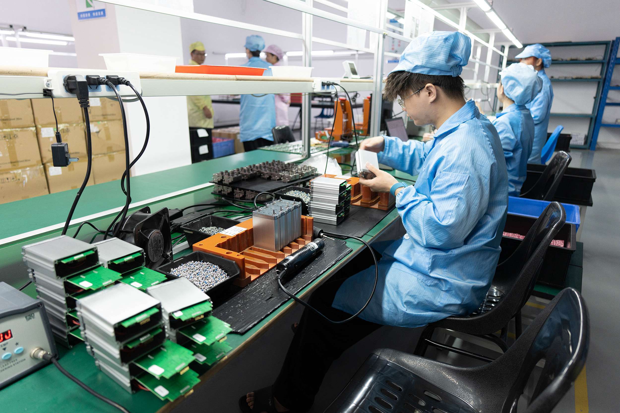
7.1 Concentrated Yet Fragmented: Understanding the PCB Industry's Dual Structure
China's PCB industry exhibits what appears to be a paradoxical characteristic: at the global level, mainland China accounts for approximately 54% of global output value, with leading companies Zhen Ding Tech at approximately 12.1% global share, Suzhou Dongshan Precision at approximately 8%, and Shennan Circuits at approximately 5%; the three combined at approximately 25% mean that the Pearl River Delta and Yangtze River Delta together have built roughly half of global PCB production. Yet within China, the 2023 CR3 was only 17.79% and CR10 only 34.9% — compared to more highly concentrated material sub-sectors such as lithium battery copper foil (top three over 70%), PCB midstream remains a highly fragmented market.
The root of this dual structure lies in the economics of PCB manufacturing:
First, product diversity blocks the transmission of scale effects. Single-layer, double-layer, standard multilayer (4–8 layers), advanced HDI, FPC, and rigid-flex each have vastly different process routes, equipment requirements, and customer qualification criteria. Leading companies have built high-barrier moats in specific technology categories — Zhen Ding Tech in FPC/SLP, WUS Printed Circuit in high-speed backplanes, Shennan Circuits and Shennan Xingsen Circuit in IC substrates; but these moats do not extend to the mid-to-low-end standard 4–8 layer board market — which has low barriers, mature processes, and diffuse customers, naturally nurturing vast numbers of small and mid-size factories.
Second, geographic supply externalities create industrial belt effects. CCL, copper foil, chemicals, dry film, ink, and equipment for drilling, lithography, and plating — once dense co-location is established in an area, the survival cost of individual small PCB factories drops significantly. The thousands of small PCB factories in Shenzhen-Huizhou-Dongguan in the Pearl River Delta sustain their viability precisely by relying on this collaborative supporting ecosystem.
Third, downstream customer structures maintain a long tail of demand. Consumer electronics, industrial control, medical, and automotive sectors are filled with non-standard customization demand; small-to-medium batch prototyping orders prioritize flexibility far above price sensitivity, and the large number of specialized small and mid-size factories is actually more competitive in this context. Nationally registered PCB-related companies exceed 5,000, with over 30 listed on A-shares — a large proportion are specialized companies focused on specific downstream segments or specific technology tiers.
7.2 Layered Profiles: Tier-1 Leaders, Mid-Range Specialists, and Small-Batch Prototype Houses
To understand the PCB industrial belt ecosystem, it is first necessary to clarify the division-of-labor logic across three tiers.
Tier 1, listed leaders (annual revenue above RMB 10 billion). Representative companies include Zhen Ding Tech (002938), Suzhou Dongshan Precision (002384), Shennan Circuits (002916), and Kinwong Electronic (603228). The core characteristic of these companies is that they have accumulated extremely high-barrier process capabilities in specific technology categories — Zhen Ding Tech's FPC/SLP production lines, Shennan Circuits' advanced multilayer server boards and IC substrate lines, WUS Printed Circuit (002463)'s ultra-heavy-copper AI server backplanes — each requiring years of continuous capital expenditure in the billions of RMB to establish. These companies typically occupy the supply chains of tier-1 customers (Apple, NVIDIA ecosystem ODMs, Huawei, etc.), with stable shipment volumes, but correspondingly high dependence on individual major customers. Competition among leaders more closely resembles "each defending their lane" than "homogeneous rivalry."
Tier 2, mid-range specialists (annual revenue RMB 2–10 billion). Representative companies include Victory Giant (300476), Chongda Technology (002815), Guangdong Ellington (603328), and Bomin Electronics (603936). These companies typically focus on one or two downstream directions (automotive electronics, industrial control, communications) and have achieved a degree of technical depth in their respective niches, but have not yet advanced to high-end products (Anylayer HDI, IC substrates). Victory Giant's 2024 revenue of RMB 10.731 billion (YoY +35.31%), with gross margin of 22.72%, is the fastest-growing mid-range specialist within the Huizhou industrial belt; Chongda Technology is positioned as a small-batch platform type, covering diverse downstream segments broadly.
Tier 3, small-batch prototype houses (annual revenue tens of millions to hundreds of millions of RMB). This is the group where the "small and fragmented" characteristic is most concentrated. These companies are primarily distributed in Shenzhen (headquarters cluster) and supporting parks in Huizhou and Dongguan, specializing in rapid prototyping (24–72 hour delivery) and small-to-medium batch customization; their pricing leverage depends entirely on the upstream supporting supply chain and overflow orders from tier-1 manufacturers. Increasingly stringent environmental compliance costs are accelerating the attrition of this group — multiple small factories in Dongguan and Shenzhen have been shut down for electroplating wastewater discharge violations, effectively raising the implicit threshold for remaining companies.
7.3 Pearl River Delta: The First Pole, Approximately 60% of National Capacity
Guangdong Province's PCB capacity accounts for approximately 60% of the national total; it is the historical birthplace of China's PCB industry and the largest and most comprehensively supported manufacturing cluster in existence. Geographically, the Pearl River Delta has formed three concentric ring layers.
The core ring is centered on Shenzhen. Shenzhen is the headquarters and R&D hub for high-end PCBs; both Zhen Ding Tech and Shennan Circuits are headquartered here. The cutting edge of IC substrate R&D — including the technical decision-making for Shennan Xingsen Circuit's Guangzhou Knowledge City production line — is also concentrated in the Pearl River Delta high-end circle. Shenzhen, with its complete financial, talent, and transportation infrastructure, is the strategic high ground for virtually all large PCB listed companies; but as land and labor costs have continued to rise, large-scale volume production has long since migrated to surrounding cities.
The second ring consists of Huizhou, Dongguan, and Zhongshan. Victory Giant's main production base is in Huizhou; Zhen Ding Tech's South China volume-production core also relies on its Huizhou base. Dongguan hosts a large amount of medium-scale standard multilayer and HDI capacity and is one of the most densely packed areas for small specialist factories. Zhongshan and Zhuhai are primarily focused on consumer electronics boards, with additional expansion toward new energy vehicle PCBs. The advantage of this ring lies in the fact that CCL (Kingboard, Shengyi), electrodeposited copper foil, chemicals, and equipment suppliers are highly concentrated within a 200-kilometer radius, making individual logistics turnaround extremely short and providing the strongest nationally small-batch rapid-response capability. Disadvantages are equally clear: land costs are already 30%–50% higher than inland receiving regions; ongoing environmental compliance upgrade costs continue to rise, driving some volume production processes toward the third ring or receiving regions in Jiangxi and Hubei.
The third ring covers Qingyuan and Heyuan. With lower land and labor costs, these areas absorb standard multilayer capacity overflow from Shenzhen-Huizhou-Dongguan, serving as a "cost valley" within the Pearl River Delta, primarily focused on mid-to-low-end standard board volume production.
7.4 Yangtze River Delta: The Second Pole, Approximately 30% of National Capacity
The Yangtze River Delta PCB cluster's distinguishing characteristic is the highest density of Taiwan-based companies nationally, forming a competitive ecosystem differentiated from the private-enterprise-led system of the Pearl River Delta.
Kunshan is the core anchor for Taiwan-based PCBs in China. Unimicron, Jinpeng Electronics, and Nan Ya PCB all have large-scale capacity in Kunshan. Unimicron is the world's leading IC substrate supplier by market share (approximately 17.7%); its Kunshan factory holds a pivotal position in its global capacity footprint. Jinpeng Electronics specializes in standard multilayer boards and HDI; Nan Ya PCB is known for vehicle-grade PCBs and industrial control boards. The greatest advantage of Taiwan-based companies is that they established comprehensive upstream-downstream interface systems relatively early: CCL suppliers TUC (Taiwan Union Technology), Iteq, and Nan Ya Plastics are all co-located in the Yangtze River Delta, forming a closed loop.
Suzhou and Jiaxing are extension nodes of the Yangtze River Delta industrial belt. Compeq's factory in Jiaxing is an important capacity point oriented toward communications and server markets. Shanghai and Suzhou are primarily focused on R&D pilot production and supporting services for high-end IC substrates, attracting some Japanese and Korean electronic chemicals suppliers, forming a high-end materials supporting ecosystem.
In 2024, Zhen Ding Tech announced investment of approximately RMB 8 billion in Huai'an, Jiangsu to build a new industrial park focused on SLP, advanced HDI, and high-layer-count capacity expansion — further extending the depth of the Yangtze River Delta industrial belt into northern Jiangsu. This positioning reflects leading companies' continued confidence in the Yangtze River Delta's talent pool and industrial ecosystem, and also mirrors the spillover trend of leaders driven by Pearl River Delta land cost constraints. Cities in northern Jiangsu such as Nantong and Yancheng absorb standard board and HDI overflow from Kunshan and Suzhou, leveraging more favorable land policies and overall costs to effectively divert mid-to-low-end capacity.
7.5 Bohai Rim: The Third Pole, Less Than 5%
Tianjin, Beijing, and surrounding areas constitute China's third PCB cluster, with capacity accounting for less than 5% of the national total, but with irreplaceable attributes in specific positioning. PCB companies in this region are primarily foreign-invested or state-enterprise-affiliated companies, mainly serving high-reliability (IPC Class 3) applications in communications base stations, defense, and aerospace/aviation; yield and reliability requirements are extremely high, with batch sizes typically far smaller than consumer electronics.
The Bohai Rim PCB industry is not known for scale, but builds moats through specialty qualifications (aerospace-grade, defense-grade certifications), forming a highly customized "small-batch, high-premium" structure. As communications equipment demand grows, this region has potential for limited scale expansion in the direction of specialty communications PCBs, but is unlikely to fundamentally alter the national capacity distribution landscape.
7.6 Central and Western Receiving Regions: Emerging Industrial Belts, Rapid Expansion 2020–2025
Rising labor costs and tightening environmental compliance constraints are the two core drivers pushing PCB capacity migration to central and western China. After 2020, three main receiving hubs have formed.
Jiangxi (Ji'an, Ganzhou) has become the most important new PCB base in central-western China, receiving not only standard board capacity but already covering compute-related high-end product lines as well. Landmark projects include: Zhen Ding Tech Jiangxi Ji'an Phase 2, with investment of approximately RMB 1.75–1.9 billion, focused on compute circuit boards and planned for phased production in 2026–2027; Shengyi Technology's Jiujiang CCL project following in parallel to complete upstream support; and the Shengyi Electronics Ji'an 5G Industrial Internet smart manufacturing factory already in production. The combination of leading company downward migration and upstream coordination means Ji'an is upgrading from a simple labor-cost valley to a mid-range production base with complete industrial support.
Hubei (Huangshi) saw its PCB industry agglomeration pace noticeably accelerate in 2023–2024. In March 2024, Huangshi City collectively signed 31 industrial projects, including 5 PCB projects with aggregate investment of RMB 2.5 billion, covering multiple categories including flexible circuit boards and high-multilayer boards. Both WUS Printed Circuit and Huangshi Electronics have production capacity in Huangshi; the combination of both companies' high-speed backplane technology capabilities and Huangshi's favorable policies makes Huangshi one of the important receiving nodes for AI server PCB capacity.
Sichuan (Guanghan, Mianyang) is primarily focused on defense equipment support and consumer electronics substrates, with a relatively thin foundation, but capacity infrastructure is gradually being established under national policy guidance. Guanghan has seen relevant PCB projects land; Mianyang, leveraging its defense research resources, is exploring differentiated positioning in the specialty high-reliability PCB direction.
Overall, the core logic for central-western receiving regions is the triple overlay of "cost + policy + leader-driven pull," but compared to the Pearl River Delta and Yangtze River Delta, the degree of agglomeration of key supporting materials such as CCL and chemicals remains significantly behind; completing the supply chain will require several years.
7.7 Southeast Asia: 2024–2029 CAGR 12.4%, Not a True Substitute in the Near Term
Against the backdrop of escalating China-US trade friction, 33 of the global top-40 PCB companies have announced plans to establish production bases in Thailand, Vietnam, or Malaysia before 2026; over one-quarter of China's top-100 PCB companies plan to build factories in these regions before 2025. Southeast Asia's PCB output value is projected to reach approximately USD 10.898 billion in 2029, approximately 12.4% of global share, with a 2024–2029 CAGR of 12.4%.
Nevertheless, Southeast Asia relocation faces three practical constraints that prevent it from constituting a true substitute for China in the near term.
First, cost advantages are limited. Southeast Asia's all-in manufacturing cost is only 10–20% lower than China's — far short of the threshold needed to drive large-scale migration. Although local labor costs are lower, logistics costs, management difficulty, and infrastructure quality gaps largely offset the labor advantage.
Second, supply chain support is absent. CCL, copper foil, chemicals, and specialized equipment have almost no local supply in Southeast Asia, meaning large quantities of raw materials still need to be imported from China or Japan, with significantly lower supply chain coordination efficiency than the mature Pearl River Delta and Yangtze River Delta clusters.
Third, high-end capacity is non-replicable. Existing Southeast Asia capacity is primarily standard multilayer boards; the precision equipment operating expertise, process engineering talent pool, and quality control systems required for high-end categories such as AI server backplanes, advanced HDI, and IC substrates cannot be established in Southeast Asia in the near term.
The US imposition in 2025 of transshipment-identification tariffs on Chinese-origin electronics routed through Vietnam effectively closed off certain "pass-through" pathways, further limiting the practical tariff-reduction benefit of Southeast Asia positioning. In the medium-to-long term, as Southeast Asia supply chains gradually mature, they will primarily exert competitive pressure on China's mid-to-low-end PCB exports, while the impact on China's high-end capacity will not be decisive before 2030.
7.8 The Upstream Identification Challenge in the "Small and Fragmented" Structure
The "small and fragmented" characteristic of PCB midstream industrial belts is reflected not only in the number and distribution of manufacturers, but also in the cognitive difficulty of understanding the entire upstream supporting system.
A qualified standard multilayer board, from raw materials to delivery, involves CCL, glass fiber cloth, copper foil, electroless plating solutions, ink, dry film, and more than a dozen process steps including drilling, lithography, electroplating, and AOI inspection — with several to dozens of specialized supporting suppliers behind each step. In the direct PCB support sector alone, upstream supplier numbers run into the thousands. These supporting factories are scattered across industrial parks at all levels in the Pearl River Delta and Yangtze River Delta, with company names changing frequently and production status and scale fluctuating sharply with market cycles.
Identifying midstream PCB factories themselves is equally difficult: nationally registered PCB-related companies exceed 5,000, but the factories that are truly in production and capable of volume delivery are far fewer than the registered count; some companies retain only a shell, with actual capacity long since outsourced or idled; and different companies vary greatly in "which type of board they make" — some specialize in FPC, some only in standard FR4 multilayer, some have entered automotive board qualification tracks, and they are largely non-interchangeable with each other.
Tianxia Gongchang is built precisely in this context, with the capability to precisely identify among approximately 4.8 million active genuine factories which PCB factory is truly in production, what type of board it primarily focuses on, and what its capacity scale is — a capability that "business registration queries" and traditional directory websites cannot provide to PCB buyers and sales teams seeking genuine counterparts.
7.9 Evolution Direction of the Industrial Belt Landscape
Synthesizing the Pearl River Delta, Yangtze River Delta, Bohai Rim, and central-western receiving regions, the evolution direction of China's PCB industrial belt landscape over the next five years is broadly clear.
High-end capacity concentrating at two poles. Advanced HDI, AI server backplanes, IC substrates, and other high-end categories will continue to be centered on Shenzhen/Guangzhou Knowledge City and Shanghai/Kunshan, because the supply of process engineers and the precision equipment service response capability in these two regions are irreplaceable. What central-western receiving regions can expand is primarily mid-range standard multilayer and standard HDI capacity.
Central-western cost valleys intensifying competition. Ji'an in Jiangxi, Huangshi in Hubei, and Guanghan in Sichuan have already formed a degree of industrial support; as more leading company projects come into production, central-western bases' comprehensive competitiveness will steadily improve, while also triggering inter-regional policy competition and capacity competition.
Environmental compliance accelerating the exit of small factories. Continuously rising thresholds for electroplating and etching wastewater treatment are an important non-market force driving slow increases in industry concentration. Small factories in the Pearl River Delta and Yangtze River Delta face a structural contradiction between upgrade costs and profitability; some will be absorbed through leader-level mergers or simply exit, with the vacated market share absorbed by already-compliant mid-range specialists and large-scale leaders.
Southeast Asia diverting mid-to-low-end, not changing the high-end structure. The results of Southeast Asia positioning will gradually materialize in 2027–2030, primarily reflected as marginal declines in China's mid-to-low-end standard board export share, rather than a reshaping of the entire industry. The "manufacturing-location compliance" requirements of European and North American customers will drive some companies to maintain limited capacity in Southeast Asia to meet customer traceability requirements, but core competitiveness will remain rooted in China's domestically complete supply chain ecosystem.
Overall, the "small and fragmented" structure of China's PCB industrial belts will not fundamentally change in the near term — the three logics of technology stratification, downstream diversity, and supply externalities are not disappearing in the short run. But a structural improvement in concentration has already been set in motion: leading companies accelerating capacity expansion in high-end categories, environmental thresholds forcing smaller players out, and central-western regions absorbing standard board overflow — the three forces combined will gradually push CR10 up from its current approximately 35% during 2026–2030, moving the industrial belt from "massively fragmented" toward "stratified and orderly."
Chapter 8 Segment Deep Dives
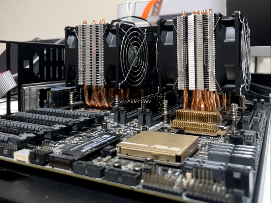
8.1 Overview of Downstream Segments
Within the approximately USD 73.3 billion global PCB market of 2024, growth-rate divergence across the six major segments has widened to a clearly visible gradient: AI servers claimed the spotlight with a near-70% year-on-year surge, automotive electronics secured its position as the second growth pole thanks to sustained EV penetration, while consumer electronics — though growing moderately — retained its status as the single largest segment by volume. The table below profiles each segment across three dimensions — market size, growth rate, and core drivers — with detailed analysis to follow.
| Segment | 2024 Global Size (est.) | YoY Growth | Core Drivers | Technical Hallmarks |
|---|---|---|---|---|
| AI Server PCB | ~USD 32 billion | +68.4% | NVIDIA Blackwell ramp, data-center capex | 28–36 layers, M8/M9/M10 CCL |
| Consumer Electronics PCB | ~USD 18.5–22 billion | Low-to-mid single digits | Handset upgrade cycles, on-device AI, foldables | SLP, Anylayer HDI, FPC |
| Automotive PCB | ~USD 10.3 billion | +12.3% | BEV penetration, ADAS, domain controllers | High-reliability multilayer, PTFE high-frequency materials |
| Industrial / Medical / Semiconductor Equipment | ~8–10% of global market, ~USD 6–7.5 billion | Steady | Automation upgrades, semiconductor localization | IPC Class 3, 40–60-layer backplanes |
| IC Substrate | ~USD 18.1 billion | +11.7% (CAGR to 2029) | Large-package AI chips, advanced packaging | FCBGA / FCCSP / BT, ABF film |
| 5G / Telecom PCB | ~28–35% of global market | Moderate recovery | Base-station expansion, 800G switches, AiP antennas | High-layer multilayer, millimeter-wave PTFE |
Note: Segments overlap to some extent (AI servers span both communications and computing); figures are parallel reference values, not strict additive totals.
8.2 AI Server PCB: A Value Revolution
8.2.1 Per-Unit Value Leap
The impact of AI servers on PCB manifests first and foremost as a qualitative leap in the PCB bill-of-materials value embedded in each completed system.
Taking the NVIDIA DGX H100 as a baseline: the per-unit PCB value is approximately USD 2,700 — roughly seven times that of a contemporaneous general-purpose server (approximately USD 335–400). This gap arises from three compounding factors: more GPU card slots and NVSwitch boards, higher layer counts on the main backplane, and high-speed CCL materials that cost several times more than FR4.
By the Blackwell-generation GB200 NVL72 rack, the value content jumped once more. A liquid-cooled rack housing 72 GPUs carries a PCB-related materials value of approximately USD 171,000 — second only to the GPUs in bill-of-materials cost and exceeding the value contribution of the CPU. The rack's complete system selling price is roughly USD 2.8–3.4 million; PCB materials account for approximately 5%–6% of system cost, a proportion unprecedented in the history of server hardware.
8.2.2 Layer Count and Material Specification Evolution
The technical parameter roadmap clearly reveals where the barrier to entry for AI server PCBs is set:
GB200 Bianca motherboard: 22-layer HDI structure, with 18 layers using M8-grade CCL and 4 core layers using M4 material, supporting 224 Gbps SerDes rates. The M8 material imposes extremely stringent control requirements on dielectric constant (Dk) and dissipation factor (Df); its cost is already significantly higher than M7-grade.
800G switch motherboards: layer counts exceed 30; WUS Printed Circuit has already mass-produced 52-layer GPU backplanes, among the highest commercially available layer counts today.
Next-generation Vera Rubin (VR200/VR300, expected H2 2026): specifications rise to 32–40 layers or more, with materials migrating to M9/M10. The unit price of M9/M10 high-speed CCL is approximately 15–20× that of ordinary FR4, meaning that even without a layer-count increase, per-unit material cost rises substantially through material-grade upgrades alone.
A concise reference for material-grade cost multiples:
- M7 (ultra-low loss): approximately 6–9× the cost of FR4; already widely used in current-generation AI servers
- M8 (primary material for GB200): cost further above M7; current mainstream specification for AI servers
- M9/M10 (Vera Rubin roadmap): approximately 15–20× FR4; mass-production still in ramp-up phase
In Blackwell-generation products, layer counts have broadly risen from the conventional 16–20 layers to 28–36 layers, and Anylayer HDI process has become standard rather than optional.
8.2.3 Market Scale and China's Three Key Beneficiaries
The global AI server PCB market reached approximately USD 32 billion in 2024, growing 68.4% year-on-year; its share of total global PCB output has risen from single digits two years ago to nearly 45%. In other words, almost half of all incremental global PCB value is coming from this single sub-segment. Another pair of figures is equally persuasive: every USD 1 of AI server revenue generates approximately 3–4× the PCB content value of a standard compute server — a multiplier effect that makes AI servers the strongest single demand driver the PCB industry has ever seen.
In the A-share market, WUS Printed Circuit (002463), Victory Giant (300476), and Shennan Circuits (002916) are the most direct beneficiaries, and each company's 2024 results confirm this assessment.
WUS Printed Circuit (002463) is the domestic core supplier of AI server motherboard backplanes, serving ODM/OEM customers such as Quanta and Wiwynn within the NVIDIA ecosystem. 2024 revenue reached RMB 13.342 billion, up 49.26% year-on-year; PCB segment gross margin rose to 35.85%, an improvement of approximately 3.4 percentage points — a gross-margin level notably above domestic general-purpose PCB peers, directly reflecting the product-mix shift toward high-layer backplanes. Orders for 28-layer-and-above advanced boards now account for more than 40% of total orders; 800G switch products are shipping in volume, and GPU-class 6-layer HDI has also passed certification and entered pre-mass-production. The company has planned an approximately RMB 4.3 billion capacity expansion project targeting AI data centers.
Victory Giant (300476) has achieved a global market-share No. 1 position in AI compute cards, data-center UBB (Universal Base Board), and switches. 2024 revenue was RMB 10.731 billion (+35.31%), with net profit attributable to the parent of RMB 1.154 billion (+71.96%) — the margin of profit growth exceeding revenue growth demonstrates that the profit-leverage effect of an improving product mix is being realized.
Shennan Circuits (002916) has followed a slightly different strategic path: in addition to benefiting directly from AI server PCB, it has extended its business chain into package substrates (IC substrates), moving toward near-semiconductor precision. Full-year 2024 revenue was RMB 17.907 billion (+32.39%), net profit attributable to the parent RMB 1.878 billion (+34.29%), IC substrate revenue RMB 3.171 billion (+37.49%), having already achieved mass production of 14-layer FCBGA and sample submission for 18/20-layer products.
All three companies point to the same signal: the per-unit value leap in AI server PCB has not only lifted overall industry sentiment, but has redefined the upper bound of "advanced multilayer board" within the Chinese mainland manufacturing ecosystem.
8.3 Consumer Electronics PCB: The Largest Segment, Structural Bifurcation
8.3.1 SLP Penetration and Technology Path
Consumer electronics — centered on smartphones — is the single largest demand source for global PCBs, accounting for approximately 25–30% of global PCB value. Ranked by product complexity, this segment exhibits a clear three-tier evolution ladder: standard multilayer HDI → Anylayer HDI → SLP (Substrate-Like PCB).
Compared with conventional HDI, SLP can reduce PCB area by approximately 30%, with line width/spacing achievable at 25–30 µm — intermediate between HDI and IC substrate. Since Apple introduced SLP with the iPhone 8/X, flagship models have continued to iterate and upgrade. The estimated smartphone shipment penetration rate for SLP technology in 2024 is approximately 16%, yet the corresponding production value share is approximately 27%, indicating that SLP products command average unit prices far above ordinary HDI — a small number of models contribute a disproportionately large share of value.
In the FPC flexible board arena, consumer electronics is also the largest application domain. A single smartphone contains an average of 10–15 FPC pieces for screen connections, camera modules, antenna feeds, and other uses. Wearables (smartwatches, fitness bands) use FPC in approximately 69% of designs, with multilayer FPC accounting for about 73% of their application mix. The adoption of foldable-screen phones further increases per-device FPC content; the ultra-thin, high-flex-cycle FPC used at the folding hinge represents the highest-barrier sub-category within FPC.
8.3.2 Zhen Ding Tech and Apple-Chain Concentration
Zhen Ding Tech (002938) is the best observation window for studying consumer electronics PCB, and also a textbook case for assessing the concentration risk of the Apple supply chain.
In 2024, Zhen Ding's revenue was RMB 35.140 billion (+9.59%), with net profit attributable to the parent of RMB 3.620 billion (+10.14%) and a gross margin of approximately 16%. Apple contributed revenue of RMB 28.793 billion, representing 81.94% of total revenue — a concentration level implying that any Apple design change or supply-chain adjustment will directly affect Zhen Ding's single-quarter results.
Notably, Zhen Ding's consumer electronics and computing board revenue reached RMB 9.754 billion (+22.30%), within which on-device AI products (PCB components supporting AI applications in the iPhone, Mac, and other devices) already account for more than 45%. This figure indicates that even traditional consumer electronics PCB manufacturers are achieving product upgrades through on-device AI penetration: the redefinition of smartphones from "consumer terminal" to "AI inference terminal" is bringing new volume-price drivers to SLP and advanced HDI. Zhen Ding is concurrently advancing its Huai'an HDI and SLP projects, laying out optical modules and other AI core areas, with cumulative investment reaching RMB 2.367 billion.
8.4 Automotive PCB: Single-Vehicle Value Reconstruction
8.4.1 Value Leap in New-Energy Vehicles
Automotive PCB was the second-fastest-growing segment in 2024, with a global market of approximately USD 10.3 billion and a CAGR of approximately 12.3% (Valuates Reports, 2025). The core logic is the amplification effect of battery electric vehicles (BEV) on per-vehicle PCB value.
A conventional entry-level internal-combustion-engine vehicle carries approximately RMB 400–600 of per-vehicle PCB value; a pure electric vehicle rises to approximately RMB 2,000+, roughly 5–6 times that of a conventional vehicle (approximately USD 100–150 vs. USD 600+ in dollar terms). The three-electric system (drive motor, electronic control, battery management) alone requires approximately 6 PCB boards totaling approximately 0.713 m², corresponding to a value of approximately RMB 640–690, accounting for approximately 43% of total vehicle PCB value — the most core source of incremental automotive PCB content.
Using the Tesla Model 3 as a reference, institutional estimates put per-vehicle PCB value at approximately RMB 1,490–1,640 — slightly below the industry median, primarily because Tesla has achieved a relatively high degree of PCB integration and domain-controller consolidation in its electronic-control systems.
The share of Chinese mainland automotive PCB in total domestic PCB output value has risen to approximately 26.9%, significantly above the global average of approximately 10–15%, directly reflecting the demand-structure difference driven by China's new-energy vehicle production scale and the world's highest EV penetration rate.
8.4.2 ADAS and Domain Controllers: Migration Toward the High End
New-energy vehicles increase the quantity of PCBs used; intelligent driving increases the technical grade. The combination of both creates a dual-flywheel growth dynamic in automotive PCB.
Millimeter-wave radar (77 GHz) PCB requires high-frequency, low-loss PTFE or modified PPE materials, with unit prices far above ordinary FR4. Domain control units (DCU) consolidate multiple electronic control units (ECU) previously scattered throughout the vehicle body onto a single high-compute board; some high-specification DCUs already require 20 or more layers, substantially higher in layer count and complexity than conventional automotive PCBs. It is forecast that ADAS applications' share of the automotive PCB market will rise to approximately 38–42% by 2026.
By contribution source: EV electrification upgrades account for approximately 25% of automotive PCB growth, ADAS system integration contributes approximately 20%, and in-vehicle infotainment (IVI) systems contribute approximately 15% — the three together covering approximately 60% of automotive PCB incremental demand.
In the domestic landscape, Kinwong Electronic (603228) leads with a platform-type capability spanning rigid PCBs and FPC, with automotive electronics as one of its key diversification outlets; Victory Giant (300476) is also advancing automotive PCB as an independent business line; Guangdong Ellington (603328) is focused on deep specialization in automotive PCB sub-segments.
Another structural feature of the automotive PCB segment is the long certification cycle. Automotive-grade PCBs typically must pass AEC-Q series reliability standards; the time from sample to mass production commonly spans 18–24 months. This is both a barrier to entry and, once certification is obtained, a moat that creates relatively high-stickiness supply relationships. Global forecasts place the automotive PCB market at approximately USD 19.2 billion by 2035, implying a 2024–2035 CAGR of approximately 8.5% — second only to AI servers and IC substrates among the six major segments, making it the medium-cycle growth segment with the strongest visibility.
8.5 Industrial, Medical, and Semiconductor Equipment: High Value, Small Volume
8.5.1 Industrial Control and Medical
Industrial control and medical together account for approximately 8–10% of global PCBs — smaller in volume than communications or consumer electronics, but this segment has two distinguishing characteristics: high added value and extremely high certification barriers.
The core requirements for industrial control PCBs are a wide operating temperature range (-40°C to 125°C), long service life (10–20 years), and IPC Class 3 high-reliability certification. Typical products include PLC controllers, variable-frequency drives, servo drivers, robotic control units, energy inverters, and industrial Ethernet switch backplanes. Expansion in energy storage, photovoltaics, and wind power has brought steady incremental demand to industrial control PCBs.
Medical PCBs likewise conform to IPC Class 3 standards; for implantable devices (pacemakers, neurostimulators), rigid-flex board materials must also exhibit biocompatibility and carry UL/FDA certification. Multilayer backplanes used in MRI/CT imaging equipment typically exceed 20 layers, with grade requirements approaching those of high-end communications PCBs. The medical sector's high entry barrier and high switching cost mean that, once certification is achieved, supply relationships are highly stable.
8.5.2 Semiconductor Equipment Backplanes
High-layer backplanes inside semiconductor equipment are among the most technically demanding PCB categories. Backplanes inside lithography systems, etch tools, and metrology instruments typically require 40–60 layers, with signal-integrity, thermal-stability, and dimensional-accuracy requirements nearly equivalent to IC substrates — though they remain within the PCB category in terms of structural form.
The supplier qualification requirements of ASML, Applied Materials (AMAT), Lam Research, and other global equipment leaders are as demanding as entering a Tier 1 automotive OEM supply chain. As domestic semiconductor equipment localization accelerates — represented by Naura Technology, Advanced Micro-Fabrication Equipment (AMEC), and Huahai Qingke — demand for domestic high-end backplanes is gradually being released. Although small in volume, this demand carries significant technology-pull value and serves as a proving ground for validating the high-end capabilities of Chinese PCB manufacturers.
8.6 IC Substrate: The Value Crown, the Largest Domestic Shortfall
8.6.1 Three Main Product Types and Applications
The IC substrate (package substrate) is the critical intermediate layer connecting bare dies to PCB motherboards, the highest-added-value, most semiconductor-adjacent category across the entire PCB supply chain, accounting for approximately 17% of global PCB output value — with a profit contribution share that is even higher.
The three mainstream types have clearly delineated roles:
FCBGA (Flip-Chip Ball Grid Array): serves CPUs, GPUs, and AI accelerator chips (Intel Sapphire Rapids, NVIDIA H100/GB200/B200, AMD MI300X, etc.). Core material is ABF film (Ajinomoto Build-up Film); current mass-production line/space is 6–7 µm, entering the 5 µm stage in 2025. Technically the most demanding, highest added value.
FCCSP (Flip-Chip Chip Scale Package): for SoCs (Qualcomm Snapdragon, Apple A-series), memory controllers, and other mobile/consumer high-performance chips. Line/space approximately 15–25 µm; materials include both ABF and BT resin.
BT substrate: based on BT (bismaleimide triazine) resin from Mitsubishi Gas Chemical (MGC); used primarily for mobile RF modules, CMOS image sensors, and low-pin-count memory packages (Flash, DRAM BGA). Technically relatively lower-barrier and the highest-volume category, currently the primary category that Chinese mainland manufacturers can produce at scale. The global BT resin supply is a duopoly controlled by Mitsubishi Gas Chemical (MGC) and Sumitomo Chemical.
The unit price of a high-end FCBGA substrate is approximately 4–5× that of an 8-layer server PCB; leading suppliers such as Ibiden have long maintained gross margins of 40–50% in this sub-segment.
8.6.2 Highly Concentrated Global Market
The global advanced IC substrate market reached approximately USD 18.1 billion in 2024, forecast to reach USD 31.5 billion by 2029, CAGR approximately 11.7%. Within this, ABF substrates (FCBGA subset) are approximately USD 4.9 billion and BT substrates approximately USD 10.5 billion.
The market is highly concentrated, with Japan, South Korea, and Taiwan together holding virtually all capacity.
| Supplier | Region | Global Share (approx.) |
|---|---|---|
| Unimicron | Taiwan | ~17.7% (2022) / ~16% (2024) |
| Nan Ya PCB | Taiwan | ~10.3% |
| Ibiden | Japan | ~9.3–9.7% |
| Samsung Electro-Mechanics (SEMCO) | South Korea | ~9.1–9.9% |
| Shinko Electric | Japan | ~8.5% |
| Top-5 combined | — | ~55% |
AT&S (Austria) is the only European company capable of mass-producing FCBGA, supplying primarily Intel and AMD, with a global share of approximately 6–9%. Ibiden holds more than 50% share in the AI-server FCBGA sub-market — the single most critical supplier of NVIDIA GPU package substrates — and has announced an approximately USD 3.3 billion capacity expansion targeting 2.5× its 2024 capacity by FY2027.
Taiwan, Japan, and South Korea combined control more than 85% of global IC substrate capacity; the materials layer (ABF film: >95% controlled by Ajinomoto; BT resin: dominated by MGC) is almost entirely in Japanese hands.
8.6.3 AI Demand Surge and ABF Supply-Demand Dynamics
The AI chip impact on IC substrates is not merely a volume multiplication — it is a qualitative escalation. NVIDIA H100/GB200/B200 all use large-format FCBGA packages; with HBM memory stacking, package footprints continue to grow. CoWoS advanced packaging technology has pushed chip die areas beyond 100 mm × 100 mm, far exceeding the mass-production yield limits of conventional FCBGA. Chip packaging layer counts have evolved from 3+3 layers to 11+11 or even 13+13 layers, causing ABF film consumption to grow geometrically.
Ajinomoto controls more than 95% of global ABF film supply and announced a price increase of approximately 30% in 2025. The supply cadence of ABF film virtually determines the global ceiling for advanced AI chip packaging capacity — the highest-leverage bottleneck node in the IC substrate supply chain.
In 2024, AI-related ABF substrate supply tightened again; Japanese manufacturers Ibiden and Shinko Electric were first to benefit, with expansion orders booked out to 2026. Meanwhile, standard server ABF substrates remained weak — a sharp bifurcation.
8.6.4 Chinese Mainland: Gap, Positioning, and the Time Window
The Chinese mainland's share of global IC substrates is approximately 4%–10% (depending on methodology) — the largest technology-level gap versus the global frontier anywhere in the PCB value chain. Shennan Circuits (002916), Xingsen Technology (002436), and Zhuhai Access are the three main domestic front-runners; together they have announced planned capacity-expansion investments of approximately RMB 16.7 billion.
Mainland manufacturers currently mass-produce primarily BT substrates. Mass-production yields for ABF FCBGA advanced products are approximately 80%–85%, compared with approximately 95% at leading international manufacturers — a roughly 10–15 percentage-point yield gap that translates into a per-unit cost disadvantage and a customer qualification barrier, making it the most critical engineering threshold to cross at present.
Xingsen Technology (002436) is advancing its two-phase FCBGA project at Guangzhou Knowledge City with a planned monthly capacity of 20 million units; major customer technical ratings and reliability verifications have been passed, and small-lot production began in Q1 2024. To support this strategic investment, the company recorded a net loss attributable to the parent of RMB 198 million in 2024 — its first annual loss in 14 years as a listed company — with cumulative investment of approximately RMB 734 million. This loss is fundamentally the unavoidable yield-ramp cost on the path to localization.
Shennan Circuits' (002916) Guangzhou Knowledge City FCBGA project involves a total investment of approximately RMB 6 billion, with a planned annual capacity at full production of approximately 200 million units; it has achieved 14-layer mass production and 18/20-layer sample submission, advancing along a technology roadmap that progressively migrates from BT to ABF FCBGA.
A meaningful breakthrough in domestic production is broadly expected to materialize gradually in 2026–2028. Behind this time window lies the synchronized unlocking of four constraints — materials, process, equipment, and certification: domestically produced ABF film substitutes have not yet achieved mass production; laser drilling machines remain heavily dependent on LPKF and Mitsubishi Electric; and the time required to obtain official Intel or NVIDIA certification is itself measured in years.
8.7 5G / Telecom PCB: An Old Engine Reignites
8.7.1 Base Stations and Network Equipment
5G telecom PCB accounts for approximately 28–35% of global downstream applications — the largest, or joint-largest, segment. Looking within, 5G base-station PCBs face clear layer-count and material requirements: Massive MIMO antenna panels require high-frequency, low-loss materials (PTFE or hybrid lamination), and the transceiver components integrated in Active Antenna Units (AAU) demand extremely high PCB signal integrity.
800G optical-interconnect switches are a core node in the data-center backbone network; their motherboards exceed 30 layers, with material grades comparable to AI server motherboards, generating incremental demand for high-layer multilayer boards in 2024–2025 that is independent of AI servers. WUS Printed Circuit's domestic 800G switch motherboards are already shipping in volume, confirming the reality of this demand.
8.7.2 AiP (Antenna-in-Package) Substrates
Millimeter-wave 5G (26 GHz / 39 GHz bands) employs Antenna-in-Package (AiP) technology, integrating the antenna array directly onto the package substrate and further blurring the boundary between PCB and package substrate. AiP substrates impose Dk/Df requirements close to those of IC substrates, yet in terms of manufacturing form still belong to PCB processing. This category remains at relatively small scale domestically, but with the acceleration of millimeter-wave 5G commercialization it is expected to become the fastest-growing sub-category within 5G telecom PCB.
Global PCB shipments for the first five months of 2025 grew approximately 7.9% year-on-year (IPC data), with May alone up as high as 21.4% year-on-year, partly attributable to communication equipment manufacturers' inventory build and the dense release of switch orders in the wave of AI adoption.
8.8 Chapter Summary
In 2024, all six major segments simultaneously revealed their driving cores: AI servers' dual volume-and-price surge is redefining the value boundary of "advanced PCB"; the per-vehicle value leap in automotive electronics makes it the most certain medium-cycle growth pole; consumer electronics, though growing modestly, still provides a stable base through its sheer volume and on-device AI penetration; industrial and medical segments use high certification barriers to protect their high-value-added territory; IC substrates remain the highest-strategic-value, largest-domestic-gap beachhead in the entire PCB chain; and 5G communications completed a moderate reboot driven by 800G upgrades and millimeter-wave commercialization.
From an investor's perspective, the opportunity profiles across the six segments differ significantly: AI servers and IC substrates are structural opportunities that transcend the cycle, but the former has entered a high-prosperity realization phase while the latter's domestic substitution cycle is still early; automotive PCB is a more steady, higher-visibility growth segment; consumer electronics largely tracks handset-upgrade and on-device-AI penetration rhythms; industrial and medical are nearly essential-demand in nature with the lowest volatility; 5G telecom is constrained by carrier capex cycles, presenting a moderate rather than explosive recovery. These six threads will be further quantified in the forecasting model of Chapter 11.
Chapter 9 Technology Evolution Trends
9.1 HDI Upgrade: From Sequential Lamination to Anylayer Interconnect
The density ceiling of printed circuit boards is determined by the precision of vias. Over the past two decades, HDI (high density interconnect) technology has completed three generations of evolution on smartphone motherboards, with each generation pushing the routeable space to a smaller scale, using the physical limits of laser drilling as its anchor.
First generation: 1+N+1 structure. One build-up layer with blind vias is added to each side of the inner core board; minimum line width/spacing is 50/50 µm. This was the standard process for mid-range smartphone motherboards in the 2010s, and the vast majority of domestic HDI capacity is concentrated here.
Second generation: 2+N+2 structure. Two build-up layers with blind vias are laminated to each side of the core; minimum line width/spacing narrows to 40/40 µm. Representative applications are flagship smartphone motherboards and high-end tablets. The process challenge lies in via-registration accuracy after two rounds of laser drilling, with more demanding yield-control requirements.
Third generation: Anylayer HDI. Any two layers across the full board can be directly interconnected via laser micro-blind vias, completely eliminating the intermediate copper-foil core that acts as a separation layer in conventional HDI, and reducing product thickness by approximately 40%. Minimum line width/spacing has been compressed to 30/30 µm; some advanced products have already reached the 25 µm mass-production node. Samsung's flagship foldable screens and Apple Watch Ultra and other wearable flagships have all adopted Anylayer architecture.
The Anylayer process has two core technical barriers. The first is laser-drilling precision: from early CO₂ laser apertures of 100 µm, evolution to combined UV-laser and CO₂-laser processing has compressed blind-via diameter to below 50 µm, approaching 30 µm; stacked-via registration error must be controlled within ±10 µm. The second is the coordinated fill of micro-vias and blind/buried vias: Anylayer requires that each blind via on every layer be completely filled by copper electroplating (Filled Via), after which vias can be stacked on top; any bubble or depression will cause reliability failure. Globally, companies capable of stable Anylayer mass production are, in mainland China, concentrated at Suzhou Dongshan Precision, Zhen Ding Tech (002938), and Shennan Circuits (002916); Japan's Nippon Mektron and Samsung Electro-Mechanics (SEMCO) are in the same tier. Domestic Anylayer capacity is still in the yield- and scale-ramp phase; reaching the scale and consistency required for stable mass production of flagship models is estimated to require approximately 2–3 more years of capacity maturation.
9.2 SLP (Substrate-Like PCB): The Transitional Form Between HDI and IC Substrate
SLP (Substrate-Like PCB) is a specialty product physically intermediate between advanced HDI and IC substrate; Apple first introduced it at scale in the iPhone X motherboard, and it has continued to iterate with each successive flagship generation.
SLP's core material switches from standard FR4 to BT (bismaleimide triazine) resin, which offers lower dielectric loss and better dimensional stability, enabling IC-substrate-grade fine-line manufacturing. The process introduces mSAP (modified semi-additive process): starting copper foil thickness does not exceed 1.5 µm; after three steps — electroless copper deposition, selective electroplating, and ultra-thin copper micro-etching — line width/spacing is compressed to 20/20 µm. This is a precision level unachievable by the subtractive process (conventional etch limit approximately 75 µm). The industry's 2025 roadmap further calls for SLP to advance toward 10/10 µm, at which point the process boundary with low-end IC substrates will virtually disappear.
From a market perspective, SLP penetration is approximately 16%, with a production-value share in flagship phones of approximately 27%. Zhen Ding Tech is the world's primary SLP supplier, deeply tied to the Apple supply chain; Shennan Circuits is catching up by leveraging mSAP process capabilities accumulated on the IC substrate side. Very few domestic companies can stably mass-produce SLP; the process certification cycle is long, and Apple's supply-chain access threshold is high, forming a dual barrier in practice. AI phones are accelerating the pace of SLP adoption in flagship models; the number of models with SLP motherboards is expected to grow more than 30% year-on-year in 2025.
9.3 IC Substrate: The Highest-Barrier Package Substrate
The IC substrate is the critical intermediate layer in flip-chip packaging, positioned between the bare die and the PCB motherboard, performing high-density rewiring and signal fan-out functions. Based on packaging form and base material, IC substrates fall into three main technology paths.
9.3.1 FCBGA Substrate: The Foundation of AI Compute Chips
FCBGA (Flip-Chip Ball Grid Array) substrate is the IC substrate category with the highest current technology barrier and largest industrial value; Intel Core, AMD EPYC, NVIDIA H100/H200/B200, and other flagship compute chips are all packaged in FCBGA form.
The core material for FCBGA substrates is ABF film (Ajinomoto Build-up Film) — a thin film that is thermally laminated layer by layer onto the core board to form structures with as many as 11+11 or even 13+13 layers. ABF film exhibits extremely low dielectric loss (Df approximately 0.003–0.005) and excellent laser-via formability, enabling precision routing at 50 µm pitch via laser drilling; it is the unavoidable bottleneck material in the current technology paradigm. Ajinomoto holds more than 95% global market share; no Chinese domestic company has completed mass-production certification of an equivalent ABF material, with domestic substitution at less than 4%.
FCBGA manufacturing also relies on mSAP or SAP processes to achieve sub-20/20 µm fine lines. Very few companies worldwide are capable of FCBGA mass production: Ibiden of Japan commands more than 50% market share in AI-server FCBGA; Unimicron holds approximately 17.7% as the leading Taiwan supplier; AT&S of Austria is the only European company with mass-production capability; Samsung Electro-Mechanics (SEMCO) holds approximately 9% share. Only Shennan Circuits and Xingsen Technology (002436) from mainland China are attempting a breakthrough.
Shennan Circuits' Guangzhou Knowledge City FCBGA line became operational in Q4 2023; 14-layer mass production is feasible, and 18/20-layer samples have been produced; Wuxi memory substrate annual capacity is 600,000 m², with total investment approximately RMB 6 billion. Xingsen Technology's FCBGA monthly capacity is approximately 2 million pieces in small-lot production; strategic cumulative investment of RMB 734 million has caused a net loss attributable to the parent of RMB 198 million in 2024 — an unavoidable cost of the domestic ramp-up phase.
Yield is the most critical barrier to FCBGA localization: mainland Chinese manufacturers' comprehensive FCBGA substrate yield is approximately 80%–85%, while mature manufacturers such as Ibiden and Unimicron achieve approximately 95% or above. The 10–15 percentage-point yield gap directly translates into persistently high per-unit costs — and is the fundamental reason why domestic FCBGA has not yet been able to enter the Tier 1 supply chains of NVIDIA and Intel at scale.
9.3.2 FCCSP Substrate: Package Substrate for Mobile SoCs
FCCSP (Flip-Chip Chip Scale Package) substrate is primarily used for mobile-side SoCs (Qualcomm, MediaTek), wireless RF chips, and memory packaging. Compared with FCBGA, FCCSP substrates are smaller, have fewer layers (typically 2–6 layers), and combine BT resin film with improved processes in pursuit of ultra-thinness and high integration density. Korea's LG Innotek is one of the leading global FCCSP suppliers; Unimicron also has large-scale capacity. Domestic FCCSP progress is faster than FCBGA, but high-end mobile SoC substrate certification still requires a lengthy 12–18 month supply-chain verification cycle.
9.3.3 BT Substrate: Mobile RF and Memory Packaging
BT substrates (BT resin substrates) use Mitsubishi Gas Chemical's (MGC) bismaleimide triazine (BT) resin as base material; more than 70% of global IC substrates use BT material, and MGC's supply of BT resin is near-monopolistic. BT substrates are widely used in mobile RF modules, CMOS image sensors, and low-pin-count memory packages (Flash, DRAM BGA) — the IC substrate category with a relatively lower technology barrier but the largest volume. Xingsen Technology has BT substrate monthly capacity of approximately 35,000 m², the most scaled domestic supplier. BT resin domestic substitution has to date not been achieved — Shengyi Technology initiated sample development around 2013 but has yet to complete mass-production certification, a covert vulnerability in China's IC substrate supply chain.
9.4 High-Speed, High-Frequency CCL: The Iterative Race Among M-Grade Materials
Data rates on AI compute backbone links have leapt from 112 Gbps to 224 Gbps, sharply elevating signal-integrity requirements for copper clad laminates (CCL). The industry uses dissipation factor (Df) as the core metric, forming an M-grade classification system that drives CCL materials toward ever-lower loss.
- M4/M5 grade (Df approximately 0.008–0.012): sub-100G switches and standard servers; domestic products from Kingboard Laminates and Shengyi Technology provide adequate coverage.
- M6 grade (Df approximately 0.005–0.008): 100G/200G GPU servers; represented by Iteq and Isola; Panasonic MEGTRON6SA series is the industry benchmark.
- M7 grade (Df approximately 0.003–0.005): AI training-server era of A100/H100; Panasonic MEGTRON7 and EMC METEORWAVE2000 are the main offerings.
- M8 grade (Df approximately 0.001–0.002): H200/GB200 and above compute platforms; Panasonic MEGTRON8 and EMC METEORWAVE4000 are in mass production; GB200 Bianca motherboards use M8 material.
- M9/M10 grade (Df < 0.001): frontier of next-generation supercomputing interconnects; in R&D and validation stage.
Shengyi Technology's (600183) S8/S9 series is the most representative domestic breakthrough in high-speed CCL: Df/Dk values have reached or approached M7/M8 equivalents; batch supply to the NVIDIA GB200/GB300 supply chain began in H2 2024; global high-speed CCL market share rose from approximately 18% in 2023 to approximately 27% in 2025; and the company is actively pursuing certifications with overseas compute customers including Google TPU, AWS, and Meta ASIC. In 2025 Shengyi plans to invest RMB 4.5 billion to expand high-performance CCL capacity to absorb the ongoing ramp in M8 mass-production demand.
The base resin for high-speed CCL has migrated from epoxy systems to PPO/PPE (polyphenylene oxide/ether) systems. PPO/PPE dielectric constant is as low as 2.3–2.5, far superior to FR-4, and is the core formulation material for M6/M7/M8-grade CCL. Domestic Hongheng Electronics' (603002) PPO downstream products have passed Intel certification reference testing, but high-purity electronic-grade PPO/PPE feedstock still relies heavily on Asahi Kasei, SABIC/GE — an import dependency not yet broken.
PTFE (polytetrafluoroethylene)-based CCL is another path: Dk approximately 2.2, Df below 0.001, widely used in 5G millimeter-wave base stations, satellite communications, and military radar where loss must be minimized. Rogers RT/duroid-series PTFE boards cost 15–20× FR4 and are difficult to process; domestic substitution rates are extremely low. Hybrid stack-ups (PTFE/FR4 mixed lamination) have also appeared in high-end AI servers, using PTFE on critical high-frequency signal layers and retaining low-cost FR4 for other layers to balance performance and cost.
9.5 mSAP and SAP: The Process Foundation for Fine Lines
From HDI to SLP to IC substrate, line-width physical limits are the core constraint at each generation of technology upgrade. Conventional PCBs use the subtractive process — etching away excess copper from a full copper foil — with a minimum line width limit of approximately 75 µm. When target line widths drop below 40 µm, undercut effects in the subtractive process cause ragged line edges and rapid yield deterioration.
- mSAP (modified semi-additive process): starting copper foil thickness does not exceed 1.5 µm; electroless copper covers the substrate, followed by photolithography, selective electroplating, and ultra-thin copper etching to achieve fine lines; mass production has reached line width/spacing of 20/20 µm; currently in volume production on SLP and low-end IC substrates.
- SAP (semi-additive process): no initial copper foil on the substrate; electroless deposition starts directly from the dielectric layer; line widths can be further reduced to 10/10 µm; in 2024 GS Swiss achieved mass production of flexible-board SAP with 10 µm line widths.
- UHDI (ultra-high-density interconnect): roadmap target of 2 µm line width in advanced IC packaging interconnect layers by 2026–2027; primarily led by Intel, Samsung, and others.
Only a handful of leading domestic companies have stable mSAP mass-production capability; SAP has no large-scale mass-production record in China. Process accumulation and yield management are the core technical barriers for domestic SLP and IC substrate catch-up, and the gap that is most difficult to rapidly close through capital investment alone in the high-end PCB localization process.
9.6 HVLP and RTF Ultra-Thin Copper Foil: The Other Half of Signal Loss
Copper foil surface roughness is an often-underestimated source of loss in high-speed signal transmission. When signal frequency exceeds 10 GHz, current tends to flow in an extremely thin surface layer of the conductor (skin effect); copper foil surface roughness (Rz) directly determines the additional signal attenuation — for every 1 µm increase in Rz, signal loss at 28 GHz increases by approximately 0.3–0.5 dB/cm. AI servers consume more than 8× as much HVLP copper foil per unit as ordinary servers.
The copper foil technology roadmap is as follows:
- Standard HTE foil (Rz 6–10 µm): ordinary multilayer PCBs.
- RTF reverse-treated foil (Rz 3–6 µm): high-frequency antennas, automotive PCBs, and mid-to-high-end consumer electronics.
- VLP very-low-profile foil (Rz 1–3 µm): high-speed servers and data-communication switches.
- HVLP foil (Rz ≤ 0.8 µm): standard specification for M7+-grade AI server PCBs.
- HVLP Gen 4/5 (Rz ≤ 0.3 µm): frontier demand for next-generation AI servers (GB200/H200); currently in R&D.
Global HVLP copper foil is dominated by Japan's Mitsui Mining & Smelting and Furukawa Electric, which together lead in top-tier AI server supply-chain certification. Domestically, Copper Crown Copper Foil (301217) is currently the only domestic company to have completed mass-production delivery of the full HVLP series (Generations 1–4); monthly shipments exceeded 100 tonnes in June 2024, and it is gradually entering the domestic AI server PCB supplier-qualification system. HVLP Gen 5 (Rz ≤ 0.3 µm) is still in the R&D phase with an uncertain mass-production window. Tongfu Microelectronics (德福科技) and Nord Copper Foil (诺德股份) are also positioning toward HVLP, but stable mass production remains some distance away. In RTF copper foil, domestic industrialization is more advanced than HVLP; Mitsui Mining & Smelting also holds a leading position in the global high-end RTF market.
9.7 FPC (Flexible PCB): Structural Increment for Foldables and Wearables
FPC (flexible printed circuit), with polyimide (PI) as its base material, serves the dual function of circuit board and conductor; it can be bent and folded, and is a foundational component in lightweight, high-integration-density consumer electronics design. The global FPC market is approximately USD 22.6 billion in 2025, forecast to reach approximately USD 56.7 billion by 2033, CAGR approximately 12%.
Foldable-screen phones are the most concentrated growth segment for FPC: more than 78% of foldable-screen models launched in 2024 integrate high-cycle-life FPC capable of withstanding more than 200,000 folding cycles, imposing far higher requirements on PI substrate fold endurance and copper foil fatigue resistance than conventional designs. Foldable-phone shipments are forecast to reach 35 million units by 2027. In wearables, approximately 69% of smartwatches and health bands use FPC for lightweight connectivity. In the new-energy vehicle sector, 67% of EVs have already adopted FPC in BMS flexible connections and as a wire-harness replacement.
COF (Chip-on-Film) and COP (Chip-on-Polymer) are derivative high-end FPC processes: COF directly flip-chip packages the driver IC onto a flexible film, widely used in OLED display driver circuits and the core flexible interconnect structure in foldable-screen display modules; COP further increases integration density and is the next-generation path for flexible hybrid electronics (FHE). Zhen Ding Tech and Suzhou Dongshan Precision (002384) are the largest-scale domestic FPC suppliers; Zhen Ding's FPC is deeply tied to Apple's consumer electronics product lines, and Suzhou Dongshan Precision's AI-related revenue already exceeds 45% of the total.
9.8 5G Millimeter-Wave and AiP PCB Substrates
The introduction of 5G millimeter-wave (28 GHz, 39 GHz, 60 GHz) bands has pushed antenna substrate dielectric-performance requirements up a level. In traditional sub-2.4 GHz bands, the dielectric loss of ordinary FR4 is still acceptable; at millimeter-wave bands, FR4's Df of approximately 0.02 is unusable, and it is necessary to switch to PTFE or low-loss LCP (liquid crystal polymer) base materials.
AiP (Antenna-in-Package) is the mainstream architecture for 5G millimeter-wave modules — integrating the RF transceiver chip and antenna array within the same package to reduce the transmission path from chip to antenna and lower interconnect losses at millimeter-wave frequencies. AiP is already widely used in 60 GHz gesture radar, 77 GHz automotive millimeter-wave radar, 94 GHz phased arrays, and 5G millimeter-wave handset RF front-end modules. AiP packaging imposes three stringent requirements on the PCB substrate: low Dk (approximately 2.2–3.0), very low Df (<0.005), and precise antenna circuit patterns (error within ±5 µm).
Hybrid stack-up is an engineering choice for controlling AiP PCB cost: mixing PTFE antenna layers with standard FR4 layers ensures RF performance while avoiding full-board high-price PTFE. Rogers/PTFE hybrid stack-up orders grew approximately 40% year-on-year in 2024, benefiting from accelerated low-earth-orbit (LEO) satellite constellation construction driving demand for both spaceborne and ground-terminal products. LCP (liquid crystal polymer) is another path for flexible 5G antenna substrates, already used in wearable 5G devices and ultra-thin antenna modules. Domestically, PTFE substrate processing and Rogers board substitution are still at an early stage, and the high-frequency millimeter-wave PCB supply chain depends significantly more on foreign materials than ordinary multilayer boards.
9.9 Six-Layer Bottleneck in Domestic Substitution
Reviewing the technology roadmaps outlined in Sections 9.1 through 9.8, China's PCB industry's domestic substitution progress faces identifiable bottlenecks at both the materials and equipment ends, summarized in six layers.
Layer 1: ABF film — complete absence. Ajinomoto controls more than 95% of global market share; no domestic company has completed mass-production certification of an equivalent material, with a domestic substitution rate of less than 4%. Ajinomoto raised prices 30% in 2025, and lead times for 14-layer ABF substrates have extended to 28 weeks. As AI chip Chiplet packaging architectures proliferate, per-chip ABF consumption continues to climb, and supply-chain initiative rests entirely with Ajinomoto. Sekisui Chemical's NX04H product is currently the only known substitution direction, but performance and certification are still catching up. Intel's exploration of glass core substrates may offer an organic alternative path by 2026–2030, but short-term demand for ABF will not decline as a result.
Layer 2: BT resin — near-monopoly. Mitsubishi Gas Chemical (MGC) dominates global BT resin supply; more than 70% of global IC substrate base materials depend on BT resin. Shengyi Technology began sample development around 2013 but has not yet achieved mass-production certification. BT substrates have large volume and a relatively lower barrier, yet the domestic production gap in the core raw material persists — a covert dependency that receives less attention than it deserves in the Chinese IC substrate supply chain.
Layer 3: HVLP Gen 5 copper foil — domestic gap. Copper Crown Copper Foil has mass-produced HVLP Generations 1–4, completing a technology breakthrough from trailing to on-par, but HVLP Gen 5 (Rz ≤ 0.3 µm) for GB200/H200-class AI servers is still in the R&D phase; Mitsui Mining & Smelting and Furukawa Electric remain the dominant suppliers to top-tier AI server copper-foil supply chains. Domestic products lag approximately one generation at the highest-end node, with an estimated catch-up window of 2–3 years.
Layer 4: Ultra-thin glass fiber — critical dimension gap. Hongheng Electronics (603256) has achieved approximately 26% global market share in ≤16 µm ultra-thin glass fiber cloth, approaching the level of Japan's Nitto Boseki in this specification; however, ≤7 µm super-ultra-thin cloth still depends on imports, one of the materials bottlenecks for high-end IC substrates and advanced SLP.
Layer 5: High-end laser drilling equipment — precision node. Han's CNC (301200) leads domestically in PCB drilling equipment and has developed CO₂ laser drilling machines supporting AI server multi-layer, high-density interconnects; however, in the highest-precision laser-via formation step for IC substrates, German LPKF and Japanese Mitsubishi Electric high-end laser drilling machines still dominate imports. The gap between domestic laser drilling machines and imports at the ordinary HDI node (≥50 µm via diameter) has narrowed substantially, but at sub-30 µm micro-via mass-production precision, there is still room to improve reliability and consistency.
Layer 6: IC substrate yield — core capability gap. The first five layers are all external supply-chain constraints; the sixth is an endogenous capability gap: mainland Chinese FCBGA manufacturers' comprehensive yield is approximately 80%–85%, versus approximately 95% for internationally mature manufacturers — a gap of approximately 10–15 percentage points. Behind yield lies the systematic accumulation of design rules, process control, and quality management systems; it cannot be bridged by substituting a single material or piece of equipment, but requires continuous production scale and stable high-end customer orders to drive the learning curve down. This gap is the most difficult threshold to cross on the path from domestic IC substrates being "technically feasible" to customers being "willing to use them."
Chapter 10 Risks and Challenges
China's PCB industry is currently at a structural inflection point: the high-prosperity cycle brought by AI servers is in sharp tension with the import dependence on advanced materials and equipment; tightening environmental regulation is forcing industry restructuring; single-customer concentration risk and cyclical demand swings are compounding each other. This chapter dissects the situation from seven dimensions — materials and equipment bottlenecks, export-control pressure, environmental constraints, customer dependence, demand cycles, competitive substitution, and raw-material costs — and uses Xingsen Technology's strategic IC substrate loss as a concrete illustration of the price of breaking into the high end.
10.1 Advanced IC Substrates: The "Material Chain" of Import Dependence
IC substrates are the PCB product family with the highest technology barrier and the lowest domestic production rate. Among all critical materials in FCBGA substrates, ABF film (Ajinomoto Build-up Film) is the core insulating layer that determines the process ceiling. Japan's Ajinomoto alone commands more than 95% of global ABF film supply; the Chinese mainland domestic substitution rate is only approximately 4%.
This monopoly produced a direct cost shock in 2025: Ajinomoto announced a price increase of approximately 30% for ABF film, directly raising material costs for domestic FCBGA substrate manufacturers. For domestic companies such as Xingsen Technology and Shennan Circuits (002916) that are still in the ramp-up phase, absorbing higher material costs before yield has reached international standards means double pressure.
On the BT resin side, Mitsubishi Gas Chemical (MGC) has long dominated the global supply of the resin system required for BT substrates. BT substrates are widely used in mobile communications SoCs and memory packaging; although technically less demanding than FCBGA, the import dependence on BT resin likewise constitutes a risk node. While domestic companies have attempted to develop alternative bismaleimide triazine resin systems, gaps in molecular-weight-distribution control and CTE matching versus MGC feedstock remain, and large-scale substitution has not yet been achieved.
Laser drilling equipment is another threshold in high-density IC substrate manufacturing. LPKF (Germany) and Mitsubishi Electric subsidiary equipment have long dominated the high-end laser drilling machine market; domestic Han's CNC (301200) and ZhengYe Technology have made breakthroughs in mid-to-low-end drilling equipment, but domestic substitution of ultra-high-precision laser direct imaging (LDI) equipment and multi-layer stacked-via alignment systems for IC substrates is still in progress.
Looking at overall domestic production rates, the Chinese mainland's IC substrate output as a share of global output is only approximately 4%–10% (depending on methodology), while the global top-three — Unimicron (Taiwan), Ibiden (Japan), and Samsung Electro-Mechanics (SEMCO, South Korea) — already combine for more than 35% market share. Across the entire advanced IC substrate value chain — from upstream ABF film, BT resin, and high-precision copper foil, through laser drilling and exposure equipment, to the final substrate product — virtually every critical link is controlled by Japanese, Taiwanese, Korean, and Western European companies; the Chinese mainland is in the complex situation of needing to simultaneously break through multiple bottleneck nodes.
Shennan Circuits currently has 16-layer-and-below FCBGA in mass production and 20-layer products in customer certification; Xingsen Technology has bulk mass-production capability for 10-layer-and-above ABF substrates. Compared with the 20-layer-and-above mass-production level of leading Taiwan and Japanese manufacturers, domestic companies generally lag approximately 2–3 generations in process maturity, and yields are in the 80%–85% range — below the industry mainstream of 95%+.
10.2 U.S. Export Controls: Dual Blocking of Equipment and Materials
The U.S. Department of Commerce BIS (Bureau of Industry and Security) export controls on China's semiconductor industry have extended from chips to advanced PCB manufacturing equipment and materials. The scope primarily covers two categories:
- Advanced lithography equipment and laser direct imaging equipment: the exposure-precision requirements for high-end IC substrates are close to those of advanced semiconductor processes; some critical equipment has been placed on export control lists, constraining domestic capacity-expansion timelines through extended procurement lead times.
- Fluorinated high-frequency dielectric materials and specialty chemicals: some specialty resins and low-dielectric-constant materials used in IC substrates and high-speed PCBs are subject to U.S.-Japan coordinated control networks, with import channels narrowing.
U.S.-Japan coordination on export controls has further reinforced the coverage of this blockade. Ajinomoto ABF film is itself of Japanese origin and is not directly listed on U.S. controls, but under U.S.-Japan coordination frameworks, technology-licensing conditions and equipment attachment clauses have already created substantive covert effects.
At the trade level, the United States in April 2025 imposed an additional 34% punitive reciprocal tariff on goods from China. Chinese PCB companies' direct exports to the U.S. were already not high in share; some companies' transhipment routes through Vietnam and Malaysia have also been narrowed by the U.S. "transit-identification tariff" mechanism. The dual equipment-and-materials constraint facing advanced IC substrates and advanced packaging is currently the most concentrated intersection of export-control impact on the PCB industry.
10.3 Environmental Pressure: A Life-or-Death Threshold for Small and Mid-Sized Manufacturers
The PCB manufacturing process involves large amounts of electroplating (copper, nickel, gold) and wet etching (corrosive solutions such as cupric chloride and ferric chloride) steps; wastewater contains copper ions, nickel ions, cyanide compounds, and other toxic and hazardous substances, posing extremely high pollution risk to groundwater and soil. China's Ministry of Ecology and Environment has implemented strict tiered discharge-permit management for the PCB industry; multiple Pearl River Delta cities have consecutively imposed moratoriums or shutdowns on non-compliant small and mid-sized PCB companies.
Rising compliance costs have an inherently "large-company-friendly" structural character: a compliant high-efficiency VOCs exhaust purification system costs tens of thousands of RMB as a one-time purchase and tens of thousands per year in operating and maintenance expenses; zero-discharge wastewater transformation, for a small factory with annual revenue below RMB 50 million, may consume a substantial fraction of its profit. This threshold is effectively accelerating the market exit of small and mid-sized factories, and is one of the important reasons for the sustained decline in the number of small and mid-sized PCB factories in the Pearl River Delta in recent years.
The capacity squeezed out has not disappeared; it has relocated wholesale to central and western China. Jiangxi Ji'an, Hubei Huangshi, and Sichuan Guanghan have successively received capacity-relocation projects from the Pearl River Delta, but the supply-chain ecosystem and skilled-worker training systems in central and western regions are still being built, and the relocation process inevitably involves a phase of reduced capacity efficiency.
In the long term, tightening environmental regulation is a double-edged sword: it eliminates high-pollution, low-efficiency small and mid-sized factories — objectively raising market concentration among compliant leaders — but also adds fixed compliance costs to the entire industry and compresses profit margins on low-to-mid-end products.
10.4 Single-Customer Concentration: Zhen Ding Tech's Apple Dependence
Zhen Ding Tech (002938) is the world's No. 1 PCB company by market share, with full-year 2024 revenue of RMB 35.140 billion; however, revenue from its largest customer (Apple) was RMB 28.793 billion, representing 81.94% of total revenue. This concentration level is far above the manufacturing industry's commonly accepted safety threshold; it means that Apple's procurement strategy, shipping cadence, and supplier-diversification decisions directly determine Zhen Ding's full-year performance.
Specific risk points include the following. First, Apple is continuously promoting PCB supplier diversification, gradually introducing competitors such as Taiwan's Career Technology, which may over time compress Zhen Ding's share. Second, if Apple's proprietary chip packaging roadmap advances SiP (System-in-Package) or higher-density integration, some FPC demand may be internalized rather than externally sourced. Third, Apple's global handset shipments are affected by the macro consumer environment and upgrade cycles — hedging against this is nearly impossible for Zhen Ding. Fourth, Apple suppliers typically face annual price reduction requirements of 3%–8%, which will directly erode gross margins in years of flat volume.
Suzhou Dongshan Precision's (002384) FPC business is similarly highly dependent on the Apple supply chain; AI end-device products account for more than 45% of its PCB revenue — structural risk similar to Zhen Ding's. At the same time, listed PCB companies in general exhibit highly concentrated top-five-customer structures; single customers exceeding 30% of revenue are not uncommon in the consumer electronics direction. From a risk-management perspective, Zhen Ding's recent acceleration in AI server backplanes and automotive PCB (combined revenue of RMB 1.03 billion in this direction in 2024, up 90.3% year-on-year) is an important initiative to actively diversify customer concentration; however, at present it accounts for less than 3%, insufficient to provide meaningful buffer.
10.5 AI Capex Cycle: Overheating Warning Behind the Boom
AI server PCB is the fastest-growing sub-segment across the entire industry in 2024–2027, with a 2024 market of approximately USD 32 billion (up 68.4% year-on-year), CAGR approximately 15.5%. This high-prosperity environment has driven a large-scale capex race among domestic PCB companies: according to Soochow Securities, planned project investment by leading domestic PCB companies for 2025–2026 totals approximately RMB 41.9 billion, concentrated primarily in two directions: high-layer boards (18 layers and above), M7/M8 high-speed CCL-compatible production lines, and IC substrates.
However, concentrated capacity expansion during a high-boom period has historically been the leading signal for overcapacity. Some institutions have already issued warnings: if AI compute demand experiences marginal deceleration in 2027–2028, the large amount of new capacity being simultaneously built domestically and overseas may create a phase of oversupply around 2028, subsequently depressing prices and profit margins for high-end PCBs.
Historical lessons are worth noting. During the consumer electronics PCB destocking cycle of 2022–2023, mid-end product capacity utilization fell rapidly from above 90% to below 70%, with across-the-board price declines. The current demand drivers for AI server PCB are a small number of hyperscale cloud companies whose capex plans are highly concentrated; once those investment schedules adjust, the contraction transmitted to the PCB end will be equally concentrated and swift.
From a demand-structure perspective, another layer of cyclical risk remains in consumer electronics: the global smartphone upgrade cycle has lengthened to approximately 3.5 years, and the marginal recovery driven by AI phones has not yet formed a structural increment sufficient to support overall demand; the laptop market is also in a relatively depressed interval ahead of AI-PC generation upgrades. Consumer electronics PCB companies still need to navigate a moderate rather than strong demand recovery in the near term.
10.6 Xingsen Technology: A Case Study of the Cash-Burn Phase in Breaking Into the High End
Xingsen Technology's (002436) net profit attributable to the parent in 2024 was -RMB 198 million — the company's first annual loss in its 14-year history as a listed company. This figure is not a loss of management control, but the inevitable cost of strategic investment: since 2022, Xingsen has cumulatively invested approximately RMB 734 million in IC substrate R&D and production-line construction at Guangzhou Knowledge City; the two-phase project has reached a monthly capacity of 20 million units, covering 10-layer-and-above ABF substrates.
The deep cause of the loss is the structural contradiction of the high-end IC substrate entry phase: below-target yield during production-line ramp-up, high depreciation and ABF film raw-material costs, long customer certification cycles (typically requiring 18–36 months before orders scale up), while end customers demand prices comparable to mature Taiwan and Japanese manufacturers. Xingsen's case demonstrates that breaking into high-end IC substrates domestically is not a purely engineering problem, but a strategic bet requiring years of sustained investment that leaves visible loss marks on financial statements.
Similar financial pressure has also appeared at Shennan Circuits: its Guangzhou Knowledge City FCBGA project involves total investment of approximately RMB 6 billion, with a planned annual capacity of approximately 200 million units; depreciation and capital costs will continue to weigh on net margins until capacity is fully released. From an industry-wide perspective, the financial cost of IC substrate localization will continue to be visible in 2025–2027 — an unavoidable phase of high-end breakthrough, not individual company operational failure.
10.7 Southeast Asian Capacity Migration: Boundaries and Timing of the Threat
Against the backdrop of sustained Sino-U.S. trade friction, PCB capacity migration to Southeast Asia has become a topic of repeated discussion. At the data level, Southeast Asian PCB output CAGR for 2024–2029 is estimated at approximately 12.4%, above the global average; 33 of the world's top-40 PCB companies have already announced plans to establish capacity in Vietnam, Thailand, or Malaysia before 2026.
However, the actual threat of migration needs to be assessed within specific constraints.
On the cost side, Southeast Asian PCB manufacturing costs are currently only approximately 10%–20% lower than China's — insufficient to create an overwhelming price-competitive advantage. On the technology side, high-layer boards (18 layers and above), high-speed CCL compatibility, IC substrates, and other high-end categories depend on a highly integrated supply-chain ecosystem that Southeast Asia cannot replicate the Pearl River Delta and Yangtze River Delta's decades of supporting infrastructure in the short term. On the tariff side, the United States has added transit-identification tariffs on Chinese-origin electronics transhipped via Vietnam; some detour routes have been blocked, reducing the expected gains from relocation arbitrage.
Overall assessment: Southeast Asian capacity migration poses limited practical threat to China's high-end PCBs before 2030, but is already beginning to create marginal competitive pressure on exports of low-to-mid-end general multilayer boards (4–8-layer FR4). In the medium to long term, if local supply chains in Southeast Asia gradually mature, China's mid-end PCB export share faces a substitution risk — one of the external drivers pushing domestic mid-end PCB manufacturers to proactively upgrade toward the high end within the current window of opportunity.
10.8 Raw Material Price Volatility: The Cost-Transmission Chain from Copper to CCL
The raw material cost structure of PCBs is highly concentrated: CCL accounts for approximately 27%–40% of PCB manufacturing cost, and copper foil in turn accounts for approximately 42% of CCL's internal cost. This creates a clear cost-transmission chain: international copper price movement → change in copper foil cost → CCL selling-price adjustment → PCB manufacturer gross-margin pressure.
Quantitatively, every 10% rise in copper prices compresses PCB company gross margins by approximately 1.5–2 percentage points. In early 2025, copper prices oscillated in the range of RMB 88,000–98,000 per tonne; CCL manufacturers have raised shipment prices multiple times; mid-stream PCB companies' ability to pass on costs depends on their pricing power with downstream customers. Large customers (such as the Apple supply chain) have rigid annual price-reduction agreement constraints; smaller-lot customers have more pricing flexibility but lower order stability.
Glass fiber cloth is also a source of volatility. Demand for the dedicated specifications of Low-DK/Low-Loss high-speed glass fiber cloth for AI servers has expanded rapidly; suppliers such as Hongheng Electronics (603256) have high-speed cloth capacity in a tight-balance situation, and price premiums have trended upward. On the resin side, specialty resins such as PPO/PTFE for high-frequency dielectric applications are constrained by specialty raw-material supply; domestic substitution is not yet complete, and import dependence creates another path for price volatility.
For mid-end PCB companies whose gross margins are already not high (typically 15%–25%), persistently elevated raw material prices compounding customer annual price-reduction requirements creates a structural double-squeeze on profit margins — one of the risk factors that small and mid-sized enterprises are most difficult to address independently.
Synthesizing all eight dimensions of this chapter, the risks facing China's PCB industry fall into two categories. The first category is structural, long-term risk, including import dependence on ABF film and key equipment, the technology embargo of export controls, and the restructuring of industry patterns by environmental compliance thresholds — these risks persist and have no prospect of near-term resolution, requiring multi-year timescales to assess breakthrough paths. The second category is cyclical and competitive risk, including the overheating warning in the AI capex boom cycle, consumer electronics upgrade-cycle fluctuations, raw-material cost swings such as copper prices, and intensifying low-end competition from Southeast Asia — these risks fluctuate with macro and industry cycles, and their impact varies significantly depending on companies' product mix and customer mix. Xingsen Technology's strategic loss is the financial imprint of actively pushing into the beachhead where the first category of risk is most concentrated, reflecting the true cost that China's PCB industry must pay on its journey from large to strong.
Chapter 11 2026–2030 Forecast: A Five-Year Window for Structural Differentiation and Domestic Breakthrough
11.1 Forecast Framework and Key Assumptions
Five-year forecasts are inherently full of uncertainty — the PCB industry especially so, given rapid technology iteration, overlapping downstream cycles, and intensifying geopolitical friction; no single scenario can capture the full picture. This chapter uses a "base case + risk case" dual-track narrative, anchoring size forecasts with institutional consensus ranges and assessing growth-rate differentiation through structural drivers.
Three premise assumptions for the base case: first, AI compute investment maintains high growth in 2026–2028, with growth rate marginally decelerating but not collapsing after 2029; second, China's NEV penetration rate continues to climb toward the 50%–60% range, with domain-controller and intelligent-driving PCB demand linearly released alongside; third, IC substrate domestic substitution achieves the crossover from trial production to scale production, led by pioneers Shennan Circuits (002916) and Xingsen Technology (002436), with sustained policy funding support.
Risk-case perturbations are concentrated in four areas: ABF film price increases or supply tightening causing IC substrate expansion costs to exceed expectations; U.S. export controls expanding to cover critical process equipment such as laser direct imaging (LDI); AI capex prematurely peaking and rapidly retreating around 2028; and Southeast Asian capacity creating effective competition against Chinese low-to-mid-end PCB exports.
11.2 Global PCB Market Forecast (2030E)
Based on aggregated assessments from Technavio, Lucintel, Mordor Intelligence, and other institutions, the global PCB market CAGR for 2026–2030 is approximately 5%–7%, with a central estimate of approximately 6%. Using approximately USD 73.3 billion in 2024 as the base, the 2030 market size range is approximately USD 110–127 billion.
The divergence between institutional forecast ranges stems primarily from differences in the scope used to count AI server PCBs, and different assumptions about the pace of consumer electronics recovery. Technavio (2025) gives a 6.2% CAGR for 2025–2030 — the more optimistic end of current institutional estimates; Frost & Sullivan gives a more conservative 4.8%. The Institute judges that the dual-volume-and-price-uplift effect of AI server PCB will continue to pull the market's center of gravity upward; a 6% central estimate under the base case is reasonable.
From a regional-structure perspective, mainland China will remain the single largest production region, with 2030 market share expected to hold in the 54%–56% range; Taiwan will maintain second place by leveraging IC substrates; Japan, despite a small share, will have extremely high unit value through Ibiden and Shinko's deep tie-in to AI compute chip packaging. Southeast Asia's share will rise from approximately 7%–8% in 2024 to approximately 10%–12%, absorbing part of the migrating low-to-mid-end capacity.
11.3 China PCB Market Forecast (2030E)
China's PCB market was approximately RMB 415.6 billion in 2024; based on aggregated projections from iMedia Research, China Business Research Institute, and the Institute's own analysis, the 2030 range is approximately RMB 560–660 billion, implying a CAGR of approximately 7%–8%.
Three logical groups support a 7%–8% CAGR (above the global 6%):
- Domestic substitution acceleration: the localization of high-value segments such as IC substrates and high-speed CCL will continuously raise the share of technology value-added in China's PCB output, delivering value growth stronger than volume growth.
- AI data-center localization: leading domestic cloud companies (Alibaba Cloud, Tencent Cloud, Huawei Cloud, ByteDance) are continuously expanding compute clusters, with high-end server PCB procurement tilting toward domestic supply chains and effectively lifting the share of high-unit-price products.
- Automotive PCB China premium: China's NEV global market share continues to rise, and domestic brands such as BYD, Huawei AITO, and Xpeng have higher intelligence levels, implying per-vehicle PCB values above the global average — a dual multiplier of "China share × high value."
Downside risk mainly comes from the consumer electronics cycle. If smartphone shipment recovery falls short of expectations, ordinary HDI and FPC markets will pull overall growth down toward the 6%–7% range.
11.4 AI Server PCB: The Highest-Growth Segment (CAGR 15.5%)
AI server PCB is the fastest-growing, most visibility-certain sub-segment within this forecast period. Verified Market Reports (2025) gives a CAGR of approximately 15.5% for 2024–2033; starting from approximately USD 1.2 billion in 2024, the 2033 market size will reach approximately USD 3.5 billion. If large hyperscale data-center PCB total consumption (motherboards, backplanes, switch boards, etc.) is calculated on a unified basis, the scale figure would be larger.
The driving factors decompose into two layers. The first is the per-unit value leap: the per-unit PCB value in an NVIDIA DGX H100 server is approximately USD 2,700 — about 7× a conventional general-purpose server; the full PCB value of a GB200 NVL72 rack is approximately USD 171,000, far exceeding CPU cost. The second is total volume expansion: global AI data-center GPU shipments are forecast to grow from approximately 5 million units in 2024 to more than 20 million units by 2028, with PCB layer counts simultaneously rising from 22 layers (GB200-generation) to 32–40 layers (Vera Rubin VR200/VR300-generation), and material grades leaping from M7/M8 to M9/M10, doubling per-unit PCB cost through material-grade upgrades alone.
The multiplicative effect of these two drivers means that AI server PCB output-value growth will significantly exceed the PCB industry overall for all of the visible next three to four years.
WUS Printed Circuit (002463) is one of the most direct domestic beneficiaries. WUS supplies 52-layer advanced backplanes to NVIDIA; 28-layer-and-above advanced boards already account for more than 40% of total orders; 2024 revenue grew 49.26% year-on-year and gross margin reached 35.85%, validating the dual volume-and-price-uplift logic. Victory Giant (300476), with a leading global position in AI compute cards and UBB (Universal Base Board), is another instance of the same logic in action.
Risk boundaries also need clear marking. If AI capex peaks around 2027–2028 and experiences greater-than-expected deceleration, high-end PCB capacity expansion will face overcapacity pressure — domestic leading companies' planned new investments for 2025–2026 total approximately RMB 41.9 billion; if demand softens, new production lines still ramping up will bear significant utilization-rate pressure.
11.5 IC Substrate Localization Path: The Long Slope from ~4% to 30%–40%
IC substrate domestic substitution is the most important structural variable within the forecast period of this report, and the proposition on which judgment differences are greatest. The Institute maps the path as follows:
| Milestone | Domestic Rate | Representative Progress |
|---|---|---|
| 2020 | ~2%–3% | Almost entirely import-dependent; mainland manufacturers only at small-scale trial production |
| 2024 | ~4%–10% (varies by methodology) | Xingsen: 10+ layer FCBGA in mass production; Shennan: 16-layer mass production, 20-layer customer certification |
| 2027E | ~15%–20% | Shennan Phase 2, Xingsen Phase 2 capacity released; ABF domestic substitute materials entering trial use |
| 2030E | ~30%–40% | Multiple companies in scale production; FCBGA yield climbing toward 90%+ |
FCBGA is the hardest sub-category to crack. In 2024, domestic ABF substrate mass-production yields were approximately 80%–85%, still 10–15 percentage points below the international benchmark of approximately 95%, with a process-generation gap of approximately 2–3 generations. Shennan Circuits' Guangzhou Knowledge City FCBGA project involves total investment of approximately RMB 6 billion, with a planned annual capacity of approximately 200 million units at full production; Xingsen Technology's two-phase Zhuhai FCBGA project has a combined monthly capacity of 20 million units; together the two companies have committed more than RMB 13 billion in capex. The Institute assesses that FCBGA domestic production rate in 2030E will be approximately 25%–30%, slightly below the overall IC substrate figure, because yield ramp-up requires time to accumulate and CoWoS advanced packaging continues to raise precision requirements for substrates.
BT substrate localization (for mobile chips and DRAM packaging) is closer to completion: companies such as Zhuhai Access already have scale mass-production capability in the BT segment, with domestic production rates already significantly higher than FCBGA; the 2030 rate is estimated at 40%–50%.
ABF film is the highest and hardest bottleneck. Japan's Ajinomoto monopolizes more than 95% of global ABF film supply, raised prices approximately 30% in 2025, and the domestic substitution rate is only approximately 4%. Huazheng New Material and Hongheng Electronics are pursuing joint development; small-lot substitution is expected to be achievable by around 2028, and by 2030 the ABF film domestic substitution rate is expected to break through 4% to above 15% — though still far below fully self-reliant levels. ABF film progress will be the single most critical variable in determining whether the IC substrate localization path can deliver on its 30%–40% target.
From an investment-output timing perspective, 2026–2027 is the critical window for validating domestic IC substrate mass production. Shennan Circuits' Guangzhou Knowledge City Phase 2 and Xingsen Technology's Zhuhai Phase 2 are both expected to come online successively during this period, adding a combined monthly capacity of more than 30 million units. If this scale can successfully ramp to 70%–80% of designed capacity, the leap from 10% to 20%+ domestic production rate will be substantially completed before 2028. Equipment localization is advancing in parallel: Han's laser drilling machines and Zhengye Technology AOI inspection equipment are both extending toward IC substrate precision specifications; localization of certain process steps can reduce dependence on U.S.-Japan equipment and also help mitigate capacity-expansion uncertainty from export controls.
11.6 Comprehensive Domestic Substitution Rate Table (2020 / 2024 / 2030E)
| Category | 2020 | 2024 | 2030E |
|---|---|---|---|
| General multilayer (4–12 layer) | ~>90% | ~>95% | Maintained; competition shifts to cost and efficiency |
| Mid-range HDI (consumer/telecom) | ~65%–70% | ~70%–75% | ~85%+ |
| SLP substrate-like PCB | ~30%–40% | ~50%–60% | ~70%–75% |
| IC substrate (overall) | ~2%–3% | ~4%–10% | ~30%–40% |
| — of which FCBGA | ~<1% | ~2%–4% | ~25%–30% |
| — of which BT substrate | ~10%–15% | ~20%–25% | ~40%–50% |
| ABF film (key material) | ~<1% | ~4% | ~15%+ |
| High-speed CCL (M7/M8) | ~5%–10% | ~20%–30% | ~50%–60% |
| HVLP copper foil | ~20%–30% | ~40%–50% | ~60%–70% |
General multilayer's domestic production rate is long past the "breakthrough" phase; subsequent competitive logic is cost, environmental compliance, and automation efficiency — not technology substitution. The genuine structural opportunities are concentrated in IC substrates and high-speed materials, the two categories still in the early stages of their ramp.
11.7 Automotive PCB: The Most Certain Long-Term Segment (CAGR 12.3%)
Global automotive PCB was approximately USD 10.3 billion in 2024; industry forecasts a 2030E CAGR of approximately 12.3% — second only to AI server PCB among all major PCB sub-segments, and with lower cyclical volatility: NEV penetration improvement is a structural trend rather than a short-term capex-driven pulse.
Per-vehicle value is the most fundamental quantitative anchor. BEV per-vehicle PCB value is approximately 5–6× that of a conventional ICE vehicle: approximately RMB 400–600 for a conventional ICE vehicle, approximately RMB 2,000+ for a BEV, and vehicles with high-compute domain controllers can exceed RMB 5,000. The three-electric system (drive motor, electronic control, battery management) contributes approximately 43% of total vehicle PCB value; the high-layer backplanes (20 layers and above) required for ADAS domain controllers are among the highest unit-price automotive-grade categories.
Looking toward 2030, two multiplier effects are operating simultaneously in the Chinese auto market: first, NEV penetration still has significant room to grow, with BEV per-vehicle value substituting ICE per-vehicle value — each additional 1 million NEVs generates approximately 5× the PCB incremental value of the combustion-engine vehicles they replace; second, the intelligence level of individual NEVs is rapidly improving, and L2+-to-L4 autonomous driving penetration is pushing per-vehicle PCB value further upward — L4 vehicles already carry per-vehicle PCB values above USD 1,500.
China's automotive PCB market was approximately RMB 21.6 billion in 2024, forecast to reach approximately RMB 78.5 billion by 2029 (China Business Research Institute, 2025), a five-year CAGR of approximately 29% — far above the global average — demonstrating that China has a fundamental basis for systematically exceeding the global growth rate in this segment.
Notably, ADAS domain-controller penetration will further push up the upper bound of per-vehicle PCB value. L2+ ADAS domain controller motherboards typically have 16–20 layers, while high-compute autonomous driving platforms targeting L4 (Huawei MDC 810, NVIDIA DRIVE Orin, etc.) already require motherboards approaching 24 layers and above, with some using high-frequency low-loss materials, where per-unit value can be 3–5× ordinary automotive-grade boards. ADAS-related PCBs are expected to rise from approximately 30% of total automotive PCB in 2026–2030 to above 40%, forming the second driver of value uplift; combined with BEV penetration growth, the dual effect will jointly pull automotive PCB market growth above the broader market pace.
Victory Giant, Guangdong Ellington (603328), Chaoyun Electronics, and other companies focused on AEC-Q100 automotive certification are currently in their volume ramp phase; 2026–2028 will be the key revenue-realization window.
11.8 FPC Foldables and Wearables: Mid-Pace Growth, Constrained by Foldable-Screen Penetration Rate
The forecast logic for the FPC sub-segment is relatively clear: foldable-screen phones are the largest incremental variable; wearables are a stable ballast.
Prismark (2023) gives a global FPC market CAGR of approximately 3.5% for 2022–2027 — mid-pace growth. But if foldable-screen handset shipments achieve rapid volume as expected in 2025–2027 — with global foldable-screen shipments forecast at approximately 120 million units in 2025 — FPC growth will be noticeably above this baseline; the Institute assesses that a phased CAGR of approximately 8%–10% is achievable, but sustainability depends on whether foldable screens can penetrate from flagship premium into mass-market.
Foldable screens pull FPC demand in two ways: per-device FPC content is approximately 3× that of an ordinary smartphone (folding hinges, inner/outer screen connections, etc. require more high-cycle FPC), with per-device FPC value approximately RMB 50–120, far above the RMB 15–30 for ordinary phones. Therefore every additional 10 million foldable-screen units shipped generates FPC incremental value roughly equivalent to the FPC demand from 30 million ordinary smartphones.
Wearable devices (smartwatches, fitness bands, medical sensors) are a more stable incremental demand source. FPC usage in wearables is approximately 69%; as health-monitoring feature density continues to rise, the FPC layer count and complexity per wearable device are also increasing, creating a moderate but persistent volume-and-price uplift dynamic.
11.9 Summary of Structural Opportunities
Taking a comprehensive 2026–2030 perspective, the PCB industry's structural opportunities unfold along four main threads:
- AI server PCB: CAGR approximately 15.5%, dual volume-and-price uplift, benefiting from continuous increases in compute density. Triple leap in layer count, material grade, and per-unit value creates a value-growth space incomparable to ordinary PCBs. WUS Printed Circuit and Victory Giant are the most direct domestic beneficiary companies.
- IC substrate domestic substitution: domestic production rate climbing from approximately 4%–10% toward 30%–40% — the single largest source of incremental value creation over five years, and also the most technically demanding and capital-intensive segment. Shennan Circuits and Xingsen Technology are the primary execution entities; ABF film substitution progress is the core variable.
- Automotive PCB: CAGR approximately 12.3%; BEV per-vehicle value 5–6× ICE vehicles, with L2+ penetration further pushing per-vehicle value higher — the growth segment with the best cycle stability.
- FPC foldables: phased CAGR approximately 8%–10%, but sustainability depends on foldable-screen mass-market penetration; wearables provide a stable floor.
Multilayer boards and ordinary HDI constitute the large-volume part of the market; growth will revert to the industry average of approximately 4%–6%. Competition in this sub-segment will continue to consolidate toward the leaders, with environmental compliance costs and automation investment thresholds jointly filtering out compliant leaders.
11.10 Investment Logic: The Division Between Alpha and Beta (Institute Perspective, Not a Stock Recommendation)
Building on the structural analysis above, the Institute summarizes the 2026–2030 PCB industry investment logic as a division between two sources of return.
Alpha opportunity: IC substrate domestic breakthrough + AI server PCB high-end capacity. Their shared characteristic is growth that exceeds the industry average — derived from structural technology upgrades rather than purely cyclical elasticity. If IC substrate domestic substitution delivers as expected, Shennan Circuits' package substrate revenue could climb from RMB 3.171 billion in 2024 to the tens-of-billions range, with significant re-rating potential; WUS Printed Circuit, if it maintains its leading position in AI server backplanes, will continue to enjoy growth rates more than double the industry average. But both face execution risk — FCBGA yield ramp-up and customer certification timelines are difficult to predict precisely, and AI server PCB capacity expansion needs to stay closely synchronized with the demand side.
Beta opportunity: multilayer/HDI cyclical elasticity. Consumer electronics and telecom base-station construction cycles determine the price and utilization-rate swings of multilayer boards and mid-range HDI; the revenue and profit of platform-type companies like Zhen Ding Tech and Kinwong Electronic display pronounced cyclical characteristics. Entering at the cycle bottom and realizing gains during the recovery-elasticity realization phase is the primary return logic for this type of company.
Key risks deserve explicit enumeration:
- AI capex premature saturation in 2027–2028: if North American hyperscale data-center investment significantly slows in 2027, high-end PCB expanded capacity will face sharp utilization-rate decline risk — specifically manifesting as reduced orders for 52-layer-and-above advanced boards and softening demand for M7/M8 CCL.
- ABF film price increases and supply management: Ajinomoto has already raised prices approximately 30% in 2025; if further increases or supply restrictions targeting Chinese manufacturers are implemented, this will directly raise IC substrate production costs, compress margins, and delay the trial-production materials consumption needed for yield ramp-up.
- Southeast Asian capacity absorption accelerating: 33 of the world's top-40 PCB companies have announced plans to build factories in Thailand, Vietnam, or Malaysia before 2026. In the near term, incomplete supply-chain ecosystems limit the impact on low-to-mid-end PCBs; but if Southeast Asian supply-chain ecosystems mature by 2028–2030, they will create effective competitive pressure on Chinese low-to-mid-end PCB exports.
- U.S. export controls expanding scope: existing controls already affect some laser drilling and exposure equipment; if future expansion covers more PCB process equipment, it will affect IC substrate expansion pace and high-end HDI production efficiency, with the core impact being extended equipment delivery cycles and time-consuming process-equivalence validation.
Synthesizing all of the above analysis, the Institute assesses that the 2026–2030 PCB industry will exhibit a clear three-tier pattern of "high-end acceleration, mid-end consolidation, domestic ramp-up": high-end AI server PCB and IC substrates drive the industry's value center of gravity upward; mid-end multilayer boards accelerate consolidation under dual environmental and cost pressure; the IC substrate localization path is long but directionally clear, with the critical nodes being the breakthrough of ABF film substitute materials and the leap of FCBGA yield from approximately 85% toward 90%+. Whether these two observable milestones are reached first will be the core judgment criterion for distinguishing the medium-to-long-term competitive positions of domestic IC substrate manufacturers.
Chapter 12 Conclusions and Institute Judgments
Distilling the entire report to a single sentence: China's PCB industry's fundamental question is how to move from the "skeleton" of manufacturing to the "crown" of value — pushing the high ground of value inch by inch from ordinary multilayer boards and HDI toward IC substrates, the hardest bone to crack.
PCBs are rarely noticed. They are hidden deep inside every smartphone, every server motherboard, every automotive domain controller — thin boards repeatedly laminated from copper foil and dielectric layers. Yet from the perspective of the electronics industry, without PCBs, there would be no pathways for signals to travel between chips. China is the world's largest PCB-producing and PCB-consuming nation; mainland China's output value in 2023 already accounted for approximately 54% of the global total, and Zhen Ding Tech has held the world's No. 1 position for multiple consecutive years with approximately 12% global market share. But beneath the word "largest," a glaring gap has always been present: the Chinese mainland's IC substrate domestic-supply rate is only approximately 4%–10%; Ajinomoto monopolizes more than 95% of global ABF film supply and raised prices 30% again in 2025; FCBGA yields are still ten percentage points below the world's best. Scale leadership coexisting with high-end lagging — this is the most truthful portrait of the industry.
The root of this gap lies not in PCB factory capacity itself, but in a few things that are further upstream and more fundamental. FCBGA uses ABF film supplied exclusively by Japan's Ajinomoto; BT resin is dominated by Japan's Mitsubishi Gas Chemical; HVLP Gen 5 copper foil's global leaders are still Japan's Mitsui Mining & Smelting; high-end laser drilling machines are still Germany's LPKF and Japan's Mitsubishi Electric. Breaking through any single upstream link is not the hard part; the hard part is passing the four gates of materials, equipment, process, and yield simultaneously. Shennan Circuits has gotten FCBGA 14-layer into mass production and 18/20-layer to sample stage; Xingsen Technology built a monthly-capacity-20-million-unit line at Guangzhou Knowledge City yet paid the price of a strategic loss of -RMB 198 million in 2024. This road is destined to burn money for a long time — and is not destined to be completed in a year or two.
But the direction of change is clear. AI servers have in one stroke lifted the per-unit PCB value to 5–10× that of ordinary servers, pushing the demand for M7/M8 high-speed copper clad laminate from "nice to have" to "cannot do without"; new-energy vehicles have pulled per-vehicle PCB value from approximately USD 100–150 to USD 600+; foldable screens and wearables have pushed FPC to the new focal point of consumer electronics. These downstream segments, overlaid with the National IC Industry Investment Fund's (Big Fund) third tranche of RMB 344 billion in policy support for integrated circuits and package substrates, have given domestic PCB manufacturers the first real foundation to "take a shot at IC substrates." WUS Printed Circuit's 2024 net profit growth of 71%, Victory Giant's 72%, Shennan Circuits' 34% — behind these numbers is the resonance of two forces: the AI tailwind and domestic substitution, in sync.
It is precisely in such a chain — with PCB mid-tier general-board factories numbering in the thousands, industrial belts spanning the Pearl River Delta and Yangtze River Delta, upstream CCL/glass-fiber/copper-foil/ink/dry-film/equipment suppliers scattered across hundreds of small and mid-sized companies, and a large recent wave of factory relocations to Jiangxi Ji'an and Hubei Huangshi — that identifying "which PCB factory is truly operating, at what scale, making what type of boards, serving which downstream customers" has become a challenge shared by upstream materials suppliers, chip design houses, module and terminal manufacturers, and procurement teams alike. Platforms like Tianxia Gongchang, which identify approximately 4.8 million truly operating factories from the mass of registered business entities, let "see the factory first, then do business" no longer depend on trial-and-error with armies of people. In an industry that is finely layered yet has highly dispersed information, the ability to see clearly is itself a competitive edge.
The PCB story is, at its core, a microcosm of China's electronics manufacturing industry: getting production volume to world No. 1 is not the hard part; the hard part is, in every layer of copper foil, every copper clad laminate, every package substrate, pushing the high ground of value forward inch by inch. This internal capability on the "skeleton" is the coursework that China's electronics industry must complete on its journey from large to strong.
Looking from the vantage point of 2026, the evolution of the industry landscape is already clearly visible. On one hand, AI servers' demand for high-layer multilayer PCBs and high-speed copper clad laminates has allowed leading domestic manufacturers to complete a structural leap in gross margins — WUS, Victory Giant, and Shennan are no longer just cyclical stocks, but growth names with structural growth attributes. On the other hand, IC substrates, the most formidable high ground, are being pushed ever further into truly deep waters — from Xingsen's cash-burn phase to Shennan's yield climb, from the Big Fund's third tranche of RMB 344 billion in ammunition to the repeated global ABF shortages, "domestic substitution" is entering real deep-water territory. Over the next five years, whoever can simultaneously produce ABF film, BT resin, HVLP Gen 5 copper foil, and ultra-thin electronic-grade glass fiber will be the one who truly captures the thickest stretch of value on the path from a domestic production rate of approximately 6% climbing toward 30%–40%. This internal-capability cultivation on the "skeleton" has passed the slogan-chanting stage; what remains is the daily hard battle across the four gates of materials, process, equipment, and customer certification.
Data Sources
Factory entity identification and in-production verification in this report are based on the Tianxia Gongchang factory database (www.tianxiagongchang.com). Industry data are drawn from the following publicly available sources and cross-verified:
- Industry research institutions: Prismark, NTI (N.T. Information), IPC, TPCA (Taiwan Printed Circuit Board Association), iMedia Research, Qianzhan Industry Research Institute, Zhiyan Consulting, Huajing Industry Research Institute, Soochow Securities, CITIC Securities, Huatai Securities, Guojin Securities, Yuanzhan Huiku, and others
- Listed company annual reports and announcements: Zhen Ding Tech (002938), Shennan Circuits (002916), WUS Printed Circuit (002463), Kinwong Electronic (603228), Xingsen Technology (002436), Victory Giant (300476), Chongda Technology (002815), Suzhou Dongshan Precision (002384), Guangdong Goworld (000823), Guangdong Ellington (603328), Bomin Electronics (603936), Jin'an Guoji (002636), Shengyi Technology (600183), Hongheng Electronics (603256), Han's CNC (301200), Kingboard Laminates (1888.HK)
- Overseas listed company financial reports: Unimicron, Ibiden (4062.T), AT&S (ATS.VI), Samsung Electro-Mechanics (009150.KS), LG Innotek (011070.KS), TTM Technologies (TTMI)
- Policy documents: MIIT "Implementation Opinions on Improving Manufacturing Reliability," "Action Plan for Stable Growth in the Machinery Industry"; National IC Industry Investment Fund (Big Fund) Phases I/II/III; NDRC "Guidance Catalogue for Industrial Structure Adjustment (2024 Edition)"; Guangdong Province special emission limits and discharge-permit system-related documents
- Industry media: Jiemian News, Securities Times, Sina Finance, Hexun, Cailian Press, SemiAnalysis, GlobalTechResearch, MarketsandMarkets, Valuates Reports, Fortune Business Insights, semibay.cn
Note: Different institutions use different methodologies for the same metric (e.g., global PCB market USD 73.3 billion vs. third-party USD 80 billion+, depending on whether PCBA assembly is included; China IC substrate domestic production rate range of 4%–10% varies by sub-category). This report has presented major discrepancies side-by-side or expressed them as ranges. Numbers relating to future forecasts are uncertain; they are provided for research reference only and do not constitute investment advice.