Executive Summary
The 2025 global outsourced semiconductor assembly and test (OSAT) market reached approximately USD 48 billion, growing 10–12% year-on-year. The principal driver is explosive demand for CoWoS and HBM advanced packaging in AI accelerators — TSMC's CoWoS monthly capacity is scaling from approximately 35,000 wafers at end-2024 to a target of 130,000 wafers by end-2026, yet remains sold out through at least mid-2026. NVIDIA alone has pre-booked 60–65% of TSMC's 2026 advanced packaging capacity.
Mainland China holds approximately 30% of global OSAT capacity, on par with Taiwan — together the two account for roughly 60% of global back-end manufacturing. JCET (Changjiang Electronics Technology) (600584) ranks third globally, with FY2025 revenue of RMB 38.87 billion; Tongfu Microelectronics (002156) ranks fourth, with FY2025 revenue of RMB 27.92 billion (+16.9%) and net profit +79.9%; Huatian Technology (002185) ranks sixth, with FY2025 revenue of RMB 17.21 billion (+19%). The three together form what this report calls the "Second Pole" of global OSAT.
Core structural tension: Mainland China OSAT commands 80–90% domestic localization in traditional wire-bond packaging and is competitive in generic advanced packaging (Fan-out / Chiplet). Tongfu has mass-produced AMD Zen 5 (3nm) Chiplet packaging at its Penang facility. Yet in CoWoS/HBM packaging — the highest-value, fastest-growing sub-segment — mainland participation is under 5%, constrained by a compound lock of equipment controls (ALD / TCB / metrology tools under U.S. EAR), process know-how gaps (3–5 year lag), and restricted HBM supply.
Core conclusions:
- Mainland China OSAT's "Second Pole" status rests on solid technical foundations in traditional and generic advanced packaging — the label is earned, not fabricated.
- Chiplet packaging is the strategic breakthrough opportunity, with Tongfu's AMD-ecosystem mass production as the clearest proof point, though independent scalability beyond AMD requires ongoing validation.
- CoWoS/HBM localization requires simultaneous resolution of three constraints; domestic ALD equipment (Naura Technology) validation for TSV applications in 2026–2027 is the single most important observable milestone.
- Under the base-case scenario, China's OSAT market reaches RMB 6,800–7,500 billion by 2030 (CAGR ~10–12%), with Chiplet/Fan-out localization rising to 35–50%.
- The 2025–2030 period will be the most structurally divergent five years in mainland China's OSAT history: advanced-packaging-capable leaders will capture AI dividend upside; traditional-packaging-focused mid-tier players face sustained margin erosion.
Chapter 1 Definitions, Classification, and the Full Supply-Chain Picture
1.1 Front-End and Back-End: The Last Mile of a Chip
Semiconductor manufacturing divides into two fundamentally different worlds. The first world exists inside wafer fabs: photolithography presses circuit patterns layer by layer into silicon; ion implantation drives dopant atoms into the crystal lattice; chemical vapor deposition fills insulation layers; atomic layer deposition (ALD) grows functional films; chemical-mechanical planarization achieves surface flatness — all of this at nanometer precision. This is front-end (Front-End) manufacturing. TSMC, Samsung, and Intel compete primarily here.
The second world lives inside packaging and test facilities. Once the front-end is complete, a wafer is densely populated with individual dies. Back-end operations (Post-End) — which is to say packaging and test — cut each die from the wafer, protect it inside a chosen package form, route electrical connections out, and subject every unit to rigorous electrical qualification. This is OSAT: Outsourced Semiconductor Assembly and Test.
For most of semiconductor industry history, back-end operations were regarded as lower-value-added — mature technology, commodity-like, price-transparent. The AI era has overturned this assessment. A CoWoS-packaged NVIDIA H100 GPU carries a packaging cost of USD 500–800 per unit, roughly 20–25% of total manufacturing cost, approaching the cost contribution of front-end wafer fabrication. TSMC's CoWoS capacity has become the most-discussed supply constraint in the global AI chip ecosystem — a fact unimaginable to any packaging professional two decades ago.
1.2 The Package-Type Spectrum: From DIP to 3D Hybrid Bonding
Package evolution represents one continuous optimization across five dimensions: footprint/pin density, thermal management, signal bandwidth and latency, manufacturing cost, and reliability. The full spectrum from historical to frontier:
Through-hole and surface-mount (DIP / QFP / SOP / BGA): Wire-bond based, mature technology. BGA moved I/O pads to the chip underside as an area array, supporting thousands of signals. FCBGA (Flip-Chip BGA) flips the die face-down, replacing gold wire with solder bumps, drastically shortening interconnect paths. These remain the workhorse formats for server CPUs, GPUs, and FPGAs.
Wafer-level packaging (WLP): All packaging steps completed before wafer singulation. Fan-in WLP keeps solder balls within the die footprint, suitable for low-pin-count analog and PMIC devices. Fan-out WLP embeds the die in a reconstituted wafer of larger area, then routes I/O beyond the die perimeter using thin-film redistribution layers (RDL). TSMC InFO, ASE FOCoS, and JCET XDFOI are all Fan-out implementations. The Apple A18 Pro AP is packaged in TSMC's latest-generation InFO at sub-2μm RDL linewidth.
SiP (System-in-Package): Multiple heterogeneous dies (processor + memory + RF + passives) integrated within a single package body. Apple Watch Series 9's S9 module, produced by ASE, integrates over a dozen dies within ~1 cm².
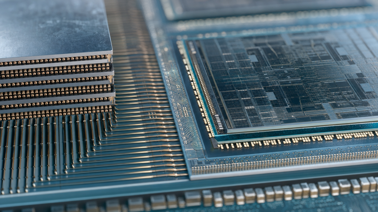
2.5D (Silicon or organic interposer): Multiple dies mounted on an interposer that provides high-density inter-die routing and TSV-based vertical I/O. TSMC CoWoS-S uses a silicon interposer with TSV and sub-1μm RDL. A single NVIDIA H100 CoWoS package carries one GH100 GPU die plus six HBM3E stacks on an ~85×85mm silicon interposer.
3D stacking (Hybrid Bonding): Dies directly bonded copper-to-copper, eliminating micro-bumps, achieving interconnect pitch down to 1–10μm — 20–50× denser than flip-chip. TSMC SoIC is the only commercially scaled Hybrid Bonding platform today.
Chiplet architecture: A design paradigm — not a single package technology — that disaggregates an SoC into functional modules (Compute Die + I/O Die + Memory Die), each fabricated at the optimal process node, then integrated via advanced packaging. AMD Zen 5, Intel Meteor Lake, and NVIDIA Blackwell B200 all exemplify Chiplet architectures.
1.3 Testing: The Underappreciated Back-End Value Driver
Testing encompasses wafer probe (CP) before singulation and final test (FT) after packaging. As advanced-node chip complexity grows exponentially, test time per unit has increased dramatically: an H100 GPU requires minutes of FT versus seconds for a consumer MCU. Teradyne UltraFlex and Advantest T8000 (HBM-specific) are the dual oligopoly in test equipment, with combined market share exceeding 70%. Domestic alternatives (Huafeng Test & Control 688004, Changchuan Technology 300604) cover analog/mixed-signal mid-tier applications but are absent in high-speed SoC and HBM test equipment. Test throughput is increasingly a hidden bottleneck: at AI-chip scale, test capacity constraints rival packaging capacity constraints.
1.4 Supply-Chain Architecture: Three Tiers, Two Dimensions
Upstream: packaging equipment (K&S, ASMPT, DISCO, Teradyne, Advantest, Besi) + materials (ABF substrates from Ibiden/Shinko; leadframes from Kangqiang Electronics; EMC from Sumitomo Bakelite) + wafer fabs (TSMC / SMIC).
Midstream: OSAT service providers. The top 10 capture ~70–75% of global market share. The bottom 300+ are regional or niche players.
Downstream: Fabless IC designers and IDMs. NVIDIA, AMD, Apple, Qualcomm, Broadcom, and HiSilicon are the order-book anchors that determine which packaging technologies get industrialized.
Value redistribution in the AI era: In a standard consumer chip, front-end manufacturing captures 60–70% of total manufacturing cost; packaging captures ~15–20%. In NVIDIA Blackwell B200, CoWoS packaging cost (USD 1,000–1,200/unit) approaches 25% of total chip manufacturing cost — compelling evidence that back-end is undergoing structural repricing.
Chapter 2 Global Competitive Landscape: Giants, Positions, and China's Rise
2.1 Market Size and Geographic Distribution
The 2025 global OSAT market totals approximately USD 48 billion. Taiwan and mainland China together account for 60% of global back-end capacity. Taiwan (30%, anchored by ASE/SPIL) and mainland China (~30%, anchored by JCET/Tongfu/Huatian) constitute the two poles. The remaining 40% is distributed across South Korea (Samsung/SK Hynix in-house + Amkor Korea base), Malaysia (Amkor Penang, Infineon, TI, Intel back-end), Philippines (Amkor, Toshiba), Vietnam (Amkor Da Nang), and the United States (Amkor Arizona + limited R&D capacity).
Advanced packaging (Fan-out / SiP / 2.5D / 3D / Chiplet) reached ~USD 45 billion globally in 2025, growing at ~8.6% CAGR toward USD 94 billion by 2034. CoWoS and HBM-related packaging within this segment is growing at 25–35% annually.
2.2 ASE Technology Holding: Global No. 1
ASE Technology Holding (3711.TW / ASX.NYSE) is the world's largest independent OSAT. Founded in 1984 in Kaohsiung, Taiwan; completed hostile acquisition of SPIL in 2015–2016 to form the current holding group. FY2025 revenue: NT$645,388M (~USD 20 billion); gross margin ~16.85%; global market share ~28–30%. LEAP (Leading-Edge Advanced Packaging) revenue scaled from USD 250M in 2023 to over USD 1.6 billion in 2025 — a 6.4× increase in three years.
2.3 Amkor Technology: Global No. 2, U.S.-Headquartered
Amkor Technology (AMKR.NASDAQ) FY2025 net sales USD 6.71 billion (+6% YoY); gross margin ~13.5%. Amkor's differentiator is geographic diversification across Korea, Malaysia, Philippines, Vietnam, Portugal, and the United States. Its Arizona facility (>USD 2B investment) serves Apple's "Made in USA" supply chain aligned with TSMC Arizona.
2.4 TSMC's Advanced Packaging: Not OSAT, but the Ecosystem Controller
TSMC's 3DIC Center — which runs CoWoS and InFO production — is not technically an OSAT, but exercises more influence over advanced packaging market dynamics than any OSAT. CoWoS capacity: ~35,000 wpm (end-2024) → ~130,000 wpm (end-2026). NVIDIA has locked ~60–65% of TSMC's 2026 advanced packaging capacity. The Chiayi AP7 campus will become the world's largest dedicated advanced packaging hub. Every major AI chip company competes for CoWoS allocation.
2.5 Global CR3 / CR6 and Mainland China's Position
| Rank | Company | Origin | FY2025 Revenue (est.) | Global Share |
|---|---|---|---|---|
| 1 | ASE | Taiwan | ~USD 20B | ~28–30% |
| 2 | Amkor | USA/Korea | ~USD 6.7B | ~14–15% |
| 3 | JCET | China | ~USD 5.3B | ~10–11% |
| 4 | Tongfu | China | ~USD 3.8B | ~7–8% |
| 5 | PTI | Taiwan | ~USD 2.0B | ~4% |
| 6 | Huatian | China | ~USD 2.4B | ~4–5% |
Mainland China CR3 (JCET + Tongfu + Huatian) collectively captures ~22–24% of global OSAT. The 2015 acquisition of Stats ChipPAC by JCET — driven by China's National IC Fund Phase 1 — was the decisive historical event that elevated mainland China from roughly 8th to 3rd globally in OSAT, entering the supply chains of Apple, Qualcomm, and Broadcom.
Chapter 3 PEST Analysis: Policy, Economic, Social, and Technology Environment
3.1 Political: National Fund III and Export Controls
The National Integrated Circuit Industry Investment Fund Phase 3 (Big Fund III) was registered in May 2024 with registered capital of RMB 344 billion, with 19 shareholders including the Ministry of Finance and major state-owned banks. Priority investment targets include advanced packaging, HBM-related materials, EUV/DUV equipment components, and EDA tools. Big Fund's stake in JCET is valued at ~RMB 6.66 billion (FY2024Q1); in Tongfu ~RMB 4.30 billion — making it the key strategic shareholder enabling long-horizon capital allocation.
U.S. EAR (Export Administration Regulations) controls have progressively tightened from 2022–2026, covering: high-end ALD equipment (ASMI, AMAT, Lam Research), thermo-compression bonder (TCB) machines (Besi), advanced wafer metrology (KLA), HBM test equipment (Advantest T8000), and hybrid bonding equipment (SET). The Netherlands and Japan have joined in coordinated controls through Wassenaar-aligned arrangements. This multi-lateral control architecture makes breakthrough timing unpredictable — the window for equipment acquisition may not reopen.
3.2 Economic: AI Capex Supercycle and Structural Demand Shift
The four hyperscalers (Microsoft, Google, Amazon, Meta) collectively spent over USD 300 billion in capex in 2025, up ~40% YoY, mostly directed at AI infrastructure. Every NVIDIA Blackwell GPU unit requires CoWoS packaging; every HBM3E stack requires precision TSV test — AI compute growth translates directly into OSAT demand.
Automotive electronics represent a structurally reliable secondary driver: content per EV is ~USD 1,000–2,000 (vs. ~USD 350–500 for ICE vehicles), growing to ~USD 2,000–3,000 by 2030. JCET's automotive electronics revenue grew +31.7% in FY2025.
3.3 Social: Engineering Talent Bifurcation
Traditional OSAT remains labor-intensive for wire-bond operations; mainland China's wage advantage vs. Taiwan (~30–40% lower) persists. However, advanced packaging is intensely engineering-reliant — globally only ~5,000–8,000 engineers with CoWoS/Hybrid Bonding production experience exist, mostly in Taiwan and Korea. Mainland China has ~500–800 such engineers, concentrated at JCET, Tongfu, and Huatian. Talent accumulation paths: university programs (SEU microelectronics, Xidian, Zhejiang), overseas Chinese returnees, and technology spillover from AMD–Tongfu collaboration.
3.4 Technology: Three Structural Drivers
Driver 1 — HBM generational escalation: HBM3E → HBM4 (H2 2026, SK Hynix-led, bandwidth >2 TB/s per die, partial Hybrid Bonding adoption) → HBM4E (2027–2028, all-Hybrid Bonding). Each generation raises TSV precision and thermal management requirements dramatically.
Driver 2 — Chiplet mass production at scale: AMD Zen 5 (3nm CCD + 6nm cIOD via Tongfu Suzhou/Penang), Intel Meteor Lake (4-tile Chiplet), NVIDIA Blackwell (NVLink-C2C dual-GPU). UCIe 1.0 standard (25μm USR bump pitch) ratified by 70+ companies including AMD, ARM, TSMC, and Samsung. UCIe 2.0 targets <10μm pitch with Hybrid Bonding support.
Driver 3 — Glass substrate and PLP as cost reduction vectors: Intel's glass substrate targets CoWoS-S silicon interposer with a larger-area, lower-cost alternative for Panther Lake (2026–2027). Panel-Level Packaging (PLP) targets 30–50% Fan-out WLP cost reduction via rectangular panel processing.
Chapter 4 China Market Size and Localization Rate Deep Dive
4.1 Total Market: RMB 4.2 Trillion in 2025
China's semiconductor packaging and test market reached approximately RMB 420 billion in 2025 (+8.8% YoY from ~RMB 386 billion in 2024). Five-year CAGR (2020–2025) of 9–11%, driven by semiconductor content growth in downstream electronics and structural localization gains. Advanced packaging (Fan-out / SiP / Chiplet / 2.5D / 3D) crossed RMB 110 billion in 2025, constituting ~26% of the total — up from ~15% in 2022.
4.2 Localization Rate by Technology Segment
| Package Type | Domestic Localization (2025 est.) | Technical Gap | Key Constraint |
|---|---|---|---|
| Traditional Wire Bond / BGA | 90%+ | Minimal | None |
| FCBGA / Flip Chip | 70–80% | ~1–2 yr | Top-tier customer certification |
| Fan-in WLP / CSP | 70–75% | ~1–2 yr | Partial equipment import dependency |
| Fan-out WLP (mid-tier) | 30–40% | ~2–3 yr | Yield / minimum linewidth |
| SiP | 20–30% | ~2–3 yr | KGD quality + system co-test |
| Chiplet generic 2.5D | 15–25% | ~2–4 yr | Large interposer yield |
| CoWoS / HBM packaging | <5% | ~3–5 yr | Equipment controls + process + supply |
| 3D Hybrid Bonding | <5% | >5 yr | Process capability absent |
4.3 Revenue Margin Structure
JCET FY2025 gross margin: 14–16%; Tongfu ~13–14%; Huatian ~13–15% — all below ASE (16.85%). The gap derives primarily from ASE's LEAP advanced packaging commanding 5–20× the ASP of traditional packaging. Margin convergence pathway = rising advanced packaging revenue share: JCET at ~70% advanced packaging share, targeting 75–80%; Huatian at ~30–35%, needing the most structural migration.
Chapter 5 Supply-Chain Anatomy: Upstream Equipment, Materials, and Downstream Clients
5.1 Upstream Equipment: The Control Points
Wire bonders: K&S (40–45% share) + ASMPT (25–30%) dominate. Domestic alternatives (Huada Semiconductor, Xinyicang 301097) serve mid-to-low tier. Not EAR-controlled.
Dicing saws: DISCO (Japan, >60% share) dominates. Laser dicing (Stealth Dicing) for ultra-thin wafers is increasingly important. Domestic player Hade Semiconductor has limited presence.
ALD equipment (for TSV insulation layers): ASMI, AMAT, Lam Research — all EAR-controlled for advanced packaging applications. Naura Technology and Advanced Micro-Fabrication Equipment (AMEC) have domestic ALD products; validation for TSV-grade applications is the critical pending milestone.
TCB (Thermo-Compression Bonding) machines: Besi (Netherlands), ASMPT — partially under enhanced Dutch scrutiny. Required for Chiplet and advanced Flip Chip. Huada Semiconductor has R&D underway.
Test equipment: Teradyne UltraFlex (40–45%) + Advantest T2000/T5000/T8000 (30–35%). T8000 (HBM-specific) EAR-controlled for China. Huafeng Test & Control has ~20–25% domestic analog test equipment share; Changchuan Technology covers handlers and some digital test equipment.
5.2 Upstream Materials: The Hidden Constraints
ABF (Ajinomoto Build-up Film): Near-monopoly supply by Ajinomoto (Japan). Required for high-end FC-BGA substrates for server CPUs/GPUs. No credible Chinese substitute yet — a materials-layer chokepoint often overlooked in advanced packaging localization discussions.
Leadframes: Kangqiang Electronics (Ningbo, 600818) and others serve mid-range wire-bond packaging with good domestic coverage.
EMC (Epoxy Molding Compound): Sumitomo Bakelite (Japan) leads. Chinese domestic players (Guoxing Optoelectronics et al.) have consumer-grade presence; automotive-grade and advanced packaging EMC still primarily imported.
Underfill: Henkel (Germany), Namics (Japan) lead for Flip Chip-grade. Domestic share is limited.
5.3 Downstream: The Order Anchors
AI accelerators (dominant incremental demand): NVIDIA Blackwell B200 (2× GPU die + 8× HBM3E, CoWoS ~100×100mm), AMD Instinct MI300X (3D stacked CPU+GPU+HBM Chiplet), Google TPU v6, Amazon Trainium 2 — all CoWoS-dependent. Single H100 CoWoS cost: ~USD 500–800. At ~2–3M AI GPU units estimated for 2025, CoWoS packaging alone represents >USD 10–20B annually.
Domestic AI chips: HiSilicon Ascend 910B/910C (Tongfu + JCET, high-spec FCBGA, no HBM yet), Cambricon MLU-590 (Tongfu), Baidu Kunlun (JCET) — domestically produced AI chips are the most geopolitically resilient demand source for mainland OSAT.
Automotive: Infineon, TI, NXP, Renesas car-chip packaging in mainland China (primarily Huatian + JCET + Sinoceratech) benefits from local-for-local supply chain logic. Horizon Robotics Journey 5/6 smart driving chips are an emerging domestic automotive packaging growth driver.
Chapter 6 Key Company Profiles
6.1 JCET (600584): Global Third, Advanced Packaging Transition
FY2025: Revenue RMB 38.87B (+8.09%, all-time high); net profit RMB 1.565B (–2.75%, "revenue up, profit down"); computing electronics +42.6%, automotive electronics +31.7%, industrial & medical +40.6%; advanced packaging revenue ~RMB 27B (all-time high). The profit compression reflects new plant ramp-up costs, rising raw material prices, and increased finance charges — all expected to normalize by FY2026–2027. XDFOI technology (2μm minimum RDL linewidth, 40×40mm max package size, mass production from H2 2022) enables Chiplet integration for domestic AI and FPGA customers. Singapore facility (JCET-ISE, ex-Stats ChipPAC) is the gateway to Tier-1 international customers.
6.2 Tongfu Microelectronics (002156): AMD Deep-Bound Chiplet Leader
FY2025: Revenue RMB 27.92B (+16.92%); net profit RMB 1.219B (+79.86%). AMD FY2025 revenue ~USD 34.6B (+34%), directly driving Tongfu volumes. AMD contribution: >80% of Tongfu Suzhou + Tongfu Penang combined revenue. Technology milestones: 7nm AMD Chiplet mass production (2019 Q4) → 5nm (2021–2022) → 3nm Penang verification and mass production (2025). Large-format Indium Bump 2.5D products reached "OSAT-leading level" per FY2025 annual report. Risk: ~80%+ AMD client concentration. Diversification into Huawei Ascend, Cambricon, etc. is the stated strategic priority.
6.3 Huatian Technology (002185): Third-Tier, in Transition
FY2025: Revenue RMB 17.21B (+19.03%); net profit RMB 711M (+15.30%). Multi-site geography: Tianshui (traditional packaging headquarters), Suzhou A (advanced packaging expansion), Shanghai (R&D). eSiFO (proprietary 8"/12" Fan-out WLP) in 5G RF front-end applications. Automotive-grade certification (AEC-Q100, IATF 16949) is the second growth curve. Key risk: lowest advanced packaging mix among the three, most exposed to traditional packaging price erosion.
6.4 Specialist Players: Jingfang Technology, Yongsi Electronics, Liyang Chip, Weice Technology, Taiji Industry
Jingfang Technology (603005): CIS/TSV WLP specialist; growing with OmniVision (Wellsemi) domestic localization. Yongsi Electronics (688362): SiP packaging for wearables and automotive; FY2025 revenue growth leading peers. Taiji Industry (600667): memory packaging tied to CXMT (ChangXin Memory) DRAM ramp. Liyang Chip (688135): analog/mixed-signal test specialist; FY2025H1 revenue +23.1%. Weice Technology (688372): digital IC final test; FY2025H1 revenue +47.5%, net profit +831% driven by AI chip test demand.
Chapter 7 Industrial Belt Geography, Factory Identification, and Global Footprint
7.1 The Jiangsu Packaging Belt: The Densest Advanced Packaging Cluster in China
Jiangyin (JCET headquarters): Largest single OSAT concentration for advanced packaging in mainland China; XDFOI Chiplet mass production line anchored here.
Nantong (Tongfu headquarters) + Suzhou Industrial Park (Tongfu Suzhou/AMD, Huatian Suzhou A, Yongsi Electronics): AMD Chiplet production center at TFAS Suzhou; Suzhou Industrial Park provides the most mature domestic packaging ecosystem (equipment service centers, material suppliers, university talent pipeline from SEU and Soochow University).
Shanghai (JCET R&D, SITRI open-platform, ASE Shanghai, Amkor Shanghai): R&D density capital; China's largest concentration of advanced packaging research institutes.
7.2 Tianshui, Gansu: Inland Packaging Base with Three-Line Heritage
Huatian Tianshui plant is mainland China's largest single-site traditional packaging base, with roots in the 1970s Third-Front construction movement. Unit labor cost ~20–30% below Jiangsu/Zhejiang; electricity cost advantage in Gansu hydro/wind-heavy grid. Annual package output capacity exceeds 200 billion units.
7.3 Factory Identification: The Invisible Long Tail
Beyond the listed OSAT leaders, mainland China has approximately 200–300 packaging-related companies — specialty chemical suppliers, leadframe manufacturers, precision tooling machined-part makers, and equipment service distributors — that are incorrectly classified in standard industrial databases. These firms' actual packaging-related activities are invisible from company names or registration codes.
Tianxia Gongchang's database of 4.8 million verified operating factories provides a supply-chain map spanning precision leadframes, packaging chemistry, test equipment agents, and cleanroom construction contractors. For a scaling OSAT, this factory-level intelligence transforms supplier sourcing from "experience-driven guesswork" to data-driven precision — identifying which local chemical supplier has semiconductor-grade purity certification, or which local precision machining shop can supply guidance frames to specification.
7.4 Overseas Footprint: Risk Dispersion Pre-Positioning
JCET Singapore (JCET-ISE, ex-Stats ChipPAC): Gateway to Tier-1 international customers (Apple, Qualcomm via supply-chain layers); geopolitically insulated from China-specific controls.
Tongfu Penang (TFAS Penang): AMD Zen 5 (3nm) Chiplet mass production validated in 2025. Demonstrates that mainland China OSAT can establish credible "non-China-made" capacity nodes for clients requiring supply chain diversification.
Huatian: No significant overseas footprint — the clearest strategic gap relative to JCET and Tongfu in international customer retention.
Chapter 8 Sub-Segment Deep Dives: Six Key Packaging Battlefields
8.1 Consumer IC Packaging: High Volume, Low Margin, Sustained Competition
USD 10–12B globally in 2025 (22–25% of total OSAT). Mainland China localization: >80%. Gross margins: 10–13% — lowest among all packaging sub-segments. The domestic structural support from Huawei/Honor recovery (Kirin 9010 ramp) and China-brand smartphone new product cycles provides a reliable volume anchor, if not a margin expansion driver.
8.2 GPU/HBM Advanced Packaging: The Hottest Segment, Almost Absent Domestically
CoWoS packaging market in 2025: estimated USD 5–8B, supply severely constrained. NVIDIA B200 packaging (2× GPU die + 8× HBM3E on ~100×100mm silicon interposer, CoWoS cost ~USD 1,000–1,200/unit) is the most technically demanding commercial package in history. Mainland domestic participation: <5%, constrained by the compound lock of EAR-controlled equipment, process know-how gap, and HBM supply restrictions. Earliest realistic national breakthrough scenario: 2029–2030 (conditional on ALD equipment validation by 2027 + domestic AI chip HBM adoption + process yield accumulation).
8.3 Memory Packaging: DRAM Cycle Bottom Passed, HBM as Separate Track
DRAM/NAND pricing recovered sharply (+80–100% and +30–50% respectively in 2025). Taiji Industry (tied to CXMT LPDDR5) is the primary mainland beneficiary. HBM packaging (SK Hynix/Samsung/Micron self-packaged, with limited external test by PTI/KYEC) is essentially inaccessible to mainland OSAT due to HBM supply export controls targeting China.
8.4 Chiplet Packaging: The National Breakthrough Opportunity
Global Chiplet packaging market: USD 3.1B (2023) → USD 6.5–8B (2025) → USD 200B (2030E), CAGR ~42.5%. Tongfu's mass-production milestones: 7nm AMD (2019Q4) → 5nm (2021) → 3nm Penang (2025). JCET XDFOI Chiplet (Interposer-less, 2μm RDL) serves domestic FPGA and AI ASIC customers. UCIe 1.0 standard enables ecosystem interoperability; mainland companies (Huawei, CASIA, Chiplets-China) participate in UCIe working groups.
8.5 Fan-Out WLP: Mainland China in the Second Tier
Global Fan-out market: USD 10B (2016) → USD 110B (2025), CAGR ~26%. Mainstream applications: mobile AP (TSMC InFO for Apple), 5G baseband assist chips, AI edge chips. JCET XDFOI: 2μm linewidth, mass production stable; gap to TSMC InFO lies in yield (>99% vs. JCET ~95–97%) and minimum linewidth (TSMC <1.5μm vs. JCET 2μm). Fan-out core technical challenge: warpage control of large reconstituted wafers — CTE mismatch between silicon (2.6 ppm/°C) and EMC (~8–12 ppm/°C) causes bowing; TSMC has optimized this over 10+ years of process data accumulation that Mainland counterparts are still catching up on.
8.6 SiP and 2.5D / 3D Stacking
SiP: Dominated by ASE (Apple Watch) at the top end; Yongsi Electronics and JCET serve mainland TWS earphones and IoT modules. Core challenge is KGD (Known Good Die) management — a bad die in SiP causes the entire package to fail at 5–20× the die cost. System-level co-test design requires early collaboration with IC design customers.
2.5D: Tongfu's Indium Bump 2.5D at "OSAT-leading level" (FY2025 report); JCET XDFOI Interposer-less 2.5D approach circumvents EAR-controlled silicon interposer TSV equipment. Still a 3–5 year gap vs. TSMC CoWoS-S in interconnect density and yield.
3D Hybrid Bonding: TSMC SoIC is the only commercial platform. Mainland R&D (CASIA, Tsinghua, HuaJin Semiconductor): laboratory-stage, commercial production >5 years away.
Chapter 9 Technology Roadmap: From HBM3E to Glass Substrates
9.1 HBM Generational Escalation
HBM3E (2024–2026 mainstream): 12–16 DRAM die stacks; ~1.28 TB/s per unit; TSV pitch ~40–55μm; die thickness <30μm. HBM4 (SK Hynix-led, H2 2026): 48GB+, >2 TB/s, partial Hybrid Bonding transition between layers, Logic Die integration (5/3nm). HBM4E (2027–2028): full Hybrid Bonding, >3 TB/s per unit — packaging complexity approaching front-end fab requirements in precision and cleanliness.
TSMC CoWoS capacity trajectory: 35,000 wpm (end-2024) → 65,000–70,000 wpm (end-2025) → 130,000 wpm (end-2026), driven by Chiayi AP7 complex coming online.
9.2 Chiplet: UCIe Standardization and Architectural Mainstream
UCIe 1.0 defines USR (25μm bump pitch, >3 Tb/s/mm bandwidth density) and SR (55μm bump pitch) interconnect tiers. UCIe 2.0 will target <10μm pitch with Hybrid Bonding support. AMD Zen 5 / EPYC Turin (3nm CCD + 6nm cIOD, mass production at Tongfu Suzhou/Penang) is the canonical Chiplet production use case for mainland OSAT. NVIDIA Blackwell (NVLink-C2C dual-GPU Chiplet + CoWoS) is the frontier reference point for where mainland OSAT aspires to be.
9.3 Glass Substrate: Intel's Long-Term Bet
Intel targets glass substrate introduction with Panther Lake (Intel 18A process, 2026–2027). Glass enables: larger package footprint (>200×200mm vs. ~85×85mm for CoWoS-S silicon interposer), lower cost than silicon, CTE tunability. TGV (Through Glass Via) fabrication faces brittleness and surface adhesion challenges. Mainland R&D (SICCAS Shanghai, SITRI): research stage only.
9.4 Key Materials: The Overlooked Localization Gap
ABF substrate material (Ajinomoto near-monopoly), high-performance underfill (Henkel/Namics), automotive-grade EMC (Sumitomo Bakelite), and ultra-high-purity specialty gases (Linde/Air Liquide/Taiyo Nippon Sanso for TSV process gases) all represent materials-layer dependencies that are distinct from — and often overlooked alongside — equipment dependencies. Big Fund III's materials investment scope (focused on photoresist, CMP pads) should be expanded to cover packaging materials if CoWoS localization is a real policy objective.
Chapter 10 Risk Matrix: Six Structural Challenges
10.1 Advanced Packaging Technology Gap: Compound Lock of Equipment Controls and Process Deficit
The CoWoS gap is not simply a technology deficit — it is a compound lock of process know-how gap (3–5 years through normal catch-up), plus equipment control amplification (EAR-controlled ALD/metrology extend the catch-up timeline by 2–3 additional years), plus yield learning dependency (without commercial volume, there is no statistical process control data; without SPC data, there is no stable yield; without stable yield, there is no commercial volume — a closed loop only broken by government-supported pilot-scale commitment). Equipment localization (Naura ALD) is the necessary and sufficient first condition; all other catch-up efforts are downstream dependencies.
10.2 U.S. EAR Escalation Risk
Controls have followed a strictly progressive path (2018 → Oct 2022 → Oct 2023 → May 2024 → 2026). The current controlled equipment list is the floor, not the ceiling of future controls. The worst-case scenario: extension of controls to mid-tier flip-chip TCB equipment (Besi) would impair current Chiplet production capability — not just CoWoS aspirations.
10.3 Traditional Packaging Price War
~200–300 OSAT operators in mainland China compete in the wire-bond / plain BGA commodity segment. JCET FY2025 ex-non-recurring net profit declined 11%, partly driven by mid-tier client pricing pressure. Mid-to-small OSAT without differentiation (automotive certification / specialty test / proprietary packaging) face sustained consolidation pressure.
10.4 HBM/AI Demand Volatility
The AI capex supercycle is real but front-loaded — hyperscaler ROI scrutiny could trigger a spending plateau in 2026–2027. HBM supply (SK Hynix + Samsung + Micron all expanding) may soften pricing by 2026–2027 even if demand remains robust. HBM test equipment overcapacity risk (Advantest T8000 orders very high in 2025) is a potential reversal signal.
10.5 Geopolitical Bifurcation
The global supply chain is dividing into a U.S./Taiwan/Japan/EU high-tech pole and a China-domestic pole. American clients are reducing direct engagement with mainland OSAT for advanced packaging (especially CoWoS-tier products). JCET Singapore and Tongfu Penang provide partial insulation but not complete coverage.
10.6 Engineering Talent Scarcity
~5,000–8,000 engineers globally with CoWoS/Hybrid Bonding mass production experience; mainland China has ~500–800. The talent gap is the second-order constraint after equipment controls: even if domestic ALD equipment is validated in 2027, without a sufficient team of TSV process engineers with production experience, yield ramp will be extremely slow. This constraint is soluble only through actual production — creating a "chicken and egg" dependency that only government-supported early commitment can break.
Chapter 11 2026–2030 Forecast: Market Projections, Localization Pathways, and Investment Logic
11.1 Global OSAT Market Forecast
Base-case scenario (probability ~55%): global OSAT market reaches USD 75–80B by 2030, CAGR ~9–11%. AI-accelerator packaging: CAGR ~25–30% (2025–2030); automotive: ~12–15%; Chiplet: ~30–40%; traditional consumer: ~3–5%.
11.2 China Domestic OSAT Market Forecast
Base-case: RMB 6,800–7,500 billion by 2030, CAGR 10–12%. Advanced packaging sub-segments: Chiplet (RMB 500–700B by 2030); Fan-out WLP (RMB 600–700B); automotive advanced packaging (RMB 400–500B); CoWoS-type (~RMB 50–150B in breakthrough scenario).
11.3 Localization Pathway: Staged Milestones
Phase 1 (2026–2027): Fan-out localization 40–50%; Chiplet (generic 2.5D) 25–35%; automotive 40–45%. Phase 2 (2028–2030): CoWoS-type localization 5–15% (breakthrough scenario); Chiplet 35–50%. The Phase 2 transition is entirely contingent on Naura ALD and domestic TCB equipment achieving production-qualified status by 2027.
11.4 Three Key Corporate Trajectories
JCET FY2026 outlook: New plant ramp-up costs normalize; advanced packaging share rising to 75–80%; computing electronics revenue continues +30–40% growth; net profit recovery toward RMB 2.0–2.5B (base case). Long-term upside: Singapore facility captures some international customer advanced packaging business as a "non-China" node.
Tongfu FY2026 outlook: AMD MI350/MI400 and EPYC Turin ramp drives volume; 3nm Chiplet yield maturation lifts ASP; non-AMD revenue (Huawei Ascend, Cambricon) growing toward 20–25% of total. Risk watch: AMD concentration and any supply chain restructuring by AMD.
Huatian FY2026 outlook: Automotive customer portfolio expansion toward 25% of total revenue; eSiFO Fan-out growth driven by 5G RF and AI edge. Core challenge: widening technology gap vs. JCET and Tongfu if advanced packaging transition remains slow.
11.5 Investment Framework: α vs. β
Industry β: AI compute demand → global OSAT valuation expansion (EV/EBITDA multiple uplift). Mainland China OSAT captures this β partially, limited by CoWoS participation gap.
Individual α sources: JCET — FY2026 net profit recovery leverage; Tongfu — AMD earnings momentum + non-AMD client expansion; Weice Technology — AI chip test demand structural surge.
Risk discounts: Geopolitical tail risk (EAR escalation → EV/EBITDA multiple compression 2–4×); AI capex slowdown (revenue estimates –20–30%); advanced packaging transition lag (valuation re-rating toward traditional manufacturing multiples).
Base-case valuation: mainland China OSAT leaders (JCET + Tongfu) fairly valued at EV/EBITDA 10–14× (vs. ASE at 12–16×, reflecting ~10–20% geopolitical discount).
Chapter 12 Conclusions: The Second Pole's Boundaries, Breakthrough Pathways, and Research Institute Assessment
12.1 Three Core Conclusions
Conclusion 1: Mainland China OSAT's "Second Pole" status in global packaging is technically earned and commercially validated — particularly in traditional packaging (wire-bond/FCBGA at 90%+ domestic localization) and generic advanced packaging (Chiplet at Tongfu-AMD scale, Fan-out at JCET XDFOI). This position is irreversible on any realistic five-year horizon.
Conclusion 2: Chiplet is the strategic breakthrough lane with real mass production proof, but independent scalability (Tongfu beyond AMD; JCET XDFOI beyond domestic FPGA/AI ASIC) remains the key validation pending. The AMD-ecosystem Chiplet know-how at Tongfu is real but is ecosystem-embedded rather than fully self-sufficient. The test: can Tongfu's 3nm Chiplet process serve non-AMD AI accelerator clients by 2027?
Conclusion 3: CoWoS/HBM localization gap of 3–5 years is not permanent but is amplified by equipment controls into a compound lock. Domestic ALD equipment (Naura) validation for TSV applications (2026–2027) is the necessary and sufficient first condition for starting the CoWoS localization clock. All other efforts — process R&D, talent accumulation, downstream HBM supply solutions — are valid but insufficient alone to start that clock.
12.2 Long-Term Structural Value
Mainland China's OSAT long-term value rests on two high-certainty structural facts:
Fact 1: The largest semiconductor consumer market is in China. Whether it is HiSilicon Kirin, Chinese EV power devices, domestic AI inference servers, or the billions of consumer chips in the global electronics supply chain — China is the permanent demand anchor for packaging services. National security-driven semiconductor localization only reinforces this anchor over time.
Fact 2: Twenty years of supply-chain depth in mainland China's packaging industrial belt is not erasable. The Jiangyin-Nantong-Suzhou-Shanghai-Tianshui-Hefei network of packaging plants, equipment distributors, chemical material suppliers, toolmakers, and university talent pipelines constitutes a structural depth that no geopolitical event can relocate or replicate within a decade.
Tianxia Gongchang's database of 4.8 million verified operating factories gives a tangible dimension to this depth: from precision leadframe manufacturers to specialty chemical suppliers, from semiconductor test equipment distributors to cleanroom precision machining contractors — this factory network is the living infrastructure of China's OSAT Second Pole.
12.3 Research Institute's Synthesis
The 2025–2030 period is the most structurally divergent five-year window in mainland China's OSAT history. Divergence between leaders (advanced packaging capable, AI dividend-leveraged) and followers (traditional packaging constrained, margin-eroded) will accelerate. The single most critical observable indicator of whether the CoWoS localization clock has started: Naura ALD equipment achieving production-line qualified yield for TSV insulation deposition at a Tier-1 OSAT by end-2027.
If that milestone is met, the 2028–2030 period will likely see initial commercial CoWoS-type packaging for domestic AI chips. If not, the compound lock extends toward 2030–2032, and the gap between mainland OSAT's "Second Pole" position and the frontier of AI-era packaging value creation will widen further before it narrows.
This report has mapped the full landscape — from DIP wire bonds to Hybrid Bonding copper-copper direct interconnect, from Tianshui assembly lines to Penang Chiplet fabs, from Big Fund III's RMB 344 billion to export-controlled ALD machines. The Second Pole stands firm. The CoWoS frontier remains the challenge of the next decade.
Data Sources and Key References
This report was compiled and analyzed by the Tianxia Gongchang Industrial Research Institute, based on the factory database and supply-chain data of the Tianxia Gongchang industrial platform (www.tianxiagongchang.com), supplemented by public disclosures, official information, and authoritative media and industry research reports. Key sources include:
- factory data platforms factory database and industrial chain data (www.tianxiagongchang.com)
- JCET (600584) FY2025 Annual Report (April 2026)
- Tongfu Microelectronics (002156) FY2025 Annual Report (April 2026)
- Huatian Technology (002185) FY2025 Annual Report (April 2026)
- ASE Technology Holding FY2025 Full Year Results (NYSE: ASX; February 2026)
- Amkor Technology FY2025 Full Year Results (NASDAQ: AMKR; February 2026)
- Jingfang Technology, Yongsi Electronics, Liyang Chip, Weice Technology, Taiji Industry FY2025 interim/annual reports
- U.S. BIS Export Control Regulations (EAR, 2022–2026 updates)
- TSMC, NVIDIA, AMD, SK Hynix FY2025 annual reports and analyst day disclosures
- Yole Développement: Advanced Packaging 2025
- TechInsights: OSAT Competitive Landscape 2025
- SEMI: Semiconductor Packaging Materials Outlook 2025
- Ministry of Industry and Information Technology (MIIT) and National IC Fund public information