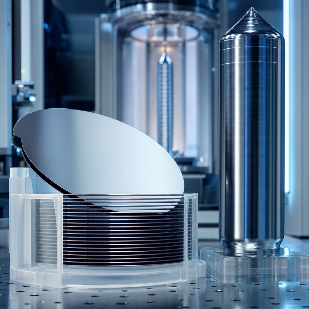
Chapter 1: 2025 Global 12-inch and 8-inch Silicon Wafer Landscape
Semiconductor silicon wafers are the physical substrate of every integrated circuit. Each logic chip, memory die, power-management IC, and image sensor must ultimately rest on a 300mm or 200mm polished, mirror-finished disc whose chemical purity (eleven nines or above) translates into crystalline purity and finally into geometric precision down to nanometer flatness. According to SEMI Industry Statistics, the global semiconductor silicon wafer market reached USD 13.6 billion in 2025, with 13.8 million MSI (million square inches) of shipments. Of this, 300mm wafers accounted for 75% by area, 200mm for 18%, and 150mm and below for under 7%. SEMI's wafer count for the year was approximately 80.5 million 300mm-equivalent wafers.
The supply concentration is arguably the highest among all semiconductor materials. Japan's Shin-Etsu Chemical holds about 28% global share, Japan's SUMCO 25%, Taiwan's GlobalWafers 15%, Germany's Siltronic 12%, South Korea's SK Siltron 11%, with the remaining ~10% divided among Chinese players (NSIG/Shanghai Xinsheng, Sien Microelectronics/Jin Ruihong, TCL Zhonghuan Lingxian, GlobalWafers Japan, Shenzhen Sino, Beijing Yanyu Semiconductor) plus a handful of second-tier overseas players. The top five oligopolies' combined share exceeds 90%—the tightest iron curtain across the entire semiconductor upstream.
The 2025 global silicon wafer market rebounded from USD 11.5 billion in 2024 to USD 13.6 billion, a year-over-year increase of about 18%. The structural recovery is driven by dual ramp of 300mm polished and epitaxial wafers—AI servers pulling HBM memory and advanced logic, automotive electrification pulling 200mm power-device wafer demand, and modest consumer-electronics recovery. SUMCO in its January 2026 earnings call revised 2026 300mm wafer shipment forecasts upward by 12%, Shin-Etsu Chemical in February 2026 by 15%, GlobalWafers in March 2026 raised epitaxial wafer guidance by 20%. The rare synchronous upward revision by all three overseas oligopolies signals that the industry has formally exited the 2023-2024 downcycle.
On the demand side, 2026 global 300mm wafer downstream consumption breaks down as: logic foundry 38%, DRAM and HBM memory 28%, 3D NAND 20%, CIS image sensors 7%, analog/power 5%, others (RF, custom ASIC) 2%. HBM is the strongest marginal driver in 2025-2026—each HBM3E stack consumes 3x or more silicon area per equivalent DDR5 capacity, and HBM4 entering 12 TB/s bandwidth pushes per-die silicon further. BloombergNEF estimates HBM-driven 300mm wafer demand growth in 2026 at around 500,000 wafers per month equivalent, translating to roughly 6 million additional polished wafer demand per month.
The 200mm wafer landscape is entirely different. 2025 global 200mm wafer shipments are approximately 7.6 million per month, with 80% serving mature-node IGBT, SiC, analog, power-management, and CIS lines. China is the largest single 200mm power-device wafer market, accounting for about 35% of global demand. 200mm purity specs are looser than 300mm—metal contamination tolerated at 1-3 ppbw, oxygen content at 10-16 ppma, single-crystal flatness up to 2.5 microns—but epitaxial layer quality, thickness tolerance, and substrate resistivity uniformity demands are actually stricter. 200mm wafer gross margins sustain at 12-18%, materially higher than 300mm polished wafer's 10%, which is why second- and third-tier Chinese wafer fabs survive long term.
In revenue-margin-share trios for 2025, the overseas oligopoly is rock stable. Shin-Etsu's Electronics Division silicon wafer revenue was JPY 580 billion (USD 3.9 billion), gross margin 28%, almost entirely from 300mm advanced logic and memory customers. SUMCO's silicon wafer revenue was JPY 380 billion (USD 2.5 billion), gross margin 24%, primarily 300mm mainstream logic. GlobalWafers consolidated revenue was TWD 71 billion (USD 2.2 billion), gross margin 26%, covering 300mm, 200mm, and 150mm fully. Siltronic generated EUR 1.5 billion (USD 1.6 billion), gross margin 15%, primary 300mm polished and epi. SK Siltron KRW 2.3 trillion (USD 1.7 billion), gross margin 18%, primary 300mm and SiC substrates.
The Chinese silicon wafer fabs' 2025 financial picture is much more bitter. NSIG (Shanghai NSIG) 2025 revenue RMB 3.6 billion, gross margin 12%, net income about RMB 300 million; Sien Microelectronics RMB 3.2 billion revenue, gross margin 20% (semiconductor segment), net income about RMB 500 million; TCL Zhonghuan Lingxian estimated wafer business revenue RMB 1.7 billion, gross margin 7%, net loss; GlobalWafers China-Suzhou TWD 4.5 billion revenue, gross margin 15%; Beijing Yanyu Semiconductor RMB 700 million revenue, gross margin 30% (FZ silicon material segment). Among Chinese wafer fabs, only Sien, Yanyu, and GlobalWafers-China can be characterized as "stable profitability." NSIG remains in its 300mm advanced epi ramp curve, TCL Zhonghuan Lingxian just started 300mm volume production.
From the supply-demand gap view, 2025 300mm polished wafer capacity utilization is about 85%—tight balance; 300mm epitaxial wafer utilization above 90%, supply-constrained; 200mm polished wafer utilization 75%, relatively loose. SUMCO in January 2026 explicitly stated: "300mm epitaxial wafer supply will remain tight through the first three quarters of 2026" and "we are seeing customer acceptance for 10-15% spot epi price increases." This is the first explicit "price increase" articulation by an overseas oligopoly in three years—a meaning far exceeding the price itself: it marks the formal pivot of the 300mm wafer cycle.
On policy and geopolitics, 2024-2026 is also the critical window for semiconductor wafer localization in China. The National Integrated Circuit Industry Investment Fund Phase III launched in March 2024 with RMB 344.4 billion, explicitly listing wafers as a "neck-blocking key category." NSIG, Sien Microelectronics, and TCL Zhonghuan Lingxian each completed at least one round of Phase III equity participation between 2024-2026, cumulatively receiving about RMB 12 billion from the Big Fund. Concurrently, indirect holdings of provincial-level integrated circuit funds (Shanghai, Anhui, etc.) in the wafer sector continue to expand. The 2025 edition of the Integrated Circuit Industry Key Materials Catalog explicitly lists 300mm polished wafers, 300mm epitaxial wafers, 300mm SOI substrates, 300mm SiGe epitaxy, and 300mm SiC substrates as priority preservation categories.
Synthesizing all of this, the 2026 Chinese semiconductor silicon wafer landscape is: overseas oligopolies hold 90% share; 300mm advanced epi is almost entirely Japan-Germany-Korea controlled; Chinese 300mm polished wafers achieve mass production at mature nodes (28nm/14nm); 300mm epi localization at advanced nodes (14nm to 7nm) is under 10%; 300mm SiGe / 300mm SOI are near zero domestic breakthrough. Every 300mm wafer localization effort must navigate the four-fold pressure of "Japan-Germany-Korea oligopolies, 18-month customer qualification cycles, hundred-billion-yuan capital outlay, and gigaton-scale electricity and water-rights constraints." The remaining thirteen chapters of this report dissect this path one wafer at a time.
The global 300mm polished wafer monthly capacity in 2025 is about 8.4 million wafers, geographically distributed as: Japan 3.2 million/month (38%), primarily at Shin-Etsu's Shirakawa-Fukushima, Takasaki-Gunma, Isobe; SUMCO's Imari, Kyushu-Ikutsuki, Yonezawa. Taiwan 1.9 million/month (23%), primarily at GlobalWafers' Zhongli, Longtan, Hukou, Taoyuan. Germany 1.2 million/month (14%), primarily at Siltronic's Freiberg, Munich-Burghausen, Singapore (the Singapore site geographically distant but Siltronic-owned). South Korea 1.05 million/month (12.5%), primarily at SK Siltron's Gumi, Cheongju. Mainland China 1.05 million/month (12.5%), primarily at NSIG's Shanghai-Lingang, Sien Microelectronics' Quzhou, TCL Zhonghuan Lingxian's Tianjin, GlobalWafers-China's Zhangjiagang and Hefei. Others (TI's US captive, Siltronic Malaysia, India Reliance soon) under 5%.
Mainland China 300mm wafer capacity was just 200,000/month in 2020, 450,000 in 2022, 800,000 in 2024, 1.05 million in 2025, projected 1.5 million in 2026. Compound growth rate of ~55%, the fastest single region globally over the past five years. But of China's 1.05 million/month 300mm capacity in 2025, polished wafers account for about 700,000 and epitaxial 350,000—epi proportion only 33%, materially below global average 50%. This asymmetric expansion "polished leads, epi lags" is the key structural bottleneck for Chinese silicon wafer industry.
China's 300mm wafer demand topology is also highly asymmetric. 2025 China's domestic 300mm wafer foundry capacity is 1.8 million/month, yielding monthly 300mm wafer demand around 1.9 million (including rework loss). Subtracting domestic capacity of 1.05 million, the import gap is 850,000/month and import dependency about 45%. This was 80% in 2020, 65% in 2022, and 50% in 2024. The expansion pace of NSIG, Sien Microelectronics, TCL Zhonghuan Lingxian, GlobalWafers-China, and Beijing Yanyu Semiconductor determines China's 300mm wafer import-dependency trajectory through 2027-2030.
Historically, in the 2010-2015 200mm wafer localization window, China traveled the full "zero to 50%" journey. But 300mm wafers must traverse a "ten percent to seventy percent" distance—a difficulty coefficient three to four times that of 200mm. Three reasons: (1) 300mm crystal pull time is 2x to 2.5x of 200mm and per-furnace capex is 3x; (2) 300mm polished wafer geometric precision demand is 3x stricter, epi 8x; (3) 300mm customer qualification cycle is 2x to 3x. This stacked difficulty compresses China's actual 300mm localization pace to "3 percentage points per year" rather than the 2010s 200mm "8 percentage points per year."
The "customer structure" of overseas wafer fabs in 2025 reads: Shin-Etsu's customers are TSMC 35%, Samsung 18%, Intel 13%, Micron 10%, SK Hynix 8%, others 15%. SUMCO: TSMC 28%, Samsung 20%, Micron 15%, Intel 10%, SK Hynix 8%, others 19%. GlobalWafers: TSMC 25%, Intel 18%, Infineon 10%, ST 8%, others 39%. Siltronic: Intel 20%, TSMC 15%, Infineon 15%, Bosch 10%, others 40%. SK Siltron: Samsung 35%, SK Hynix 28%, TSMC 10%, Intel 8%, others 19%. Overseas wafer fab customer structures align tightly with the "Big Five semiconductor giants" (TSMC, Samsung, SK Hynix, Intel, Micron)—a "five oligopolies vs five oligopolies" pattern.
Chinese wafer fab customer structures are more dispersed. NSIG 2025 customers: SMIC 28%, Hua Hong Semiconductor 15%, Yangtze Memory 10%, ChangXin Memory 8%, Hefei Nexchip 8%, China Resources Microelectronics 5%, Silan Microelectronics 4%, others 22%. Sien Microelectronics 2025: overseas (Infineon, ST, ON Semi) 30%, Hua Hong Semiconductor 15%, China Resources Micro 10%, Yangjie Tech 8%, others 37%. TCL Zhonghuan Lingxian 2025: SMIC 20%, Hua Hong Semi 15%, Hefei Nexchip 10%, Jita Semiconductor 8%, others 47%. The Chinese wafer fab customer-structure "overseas customer share" is not low—Sien's 30% overseas reflects 200mm power-device wafer's reverse "domestic wafer → overseas large customers" outflow.
Globally, semiconductor wafer share evolution is typically a glacial "1 percentage point per year." Shin-Etsu 30% share in 1995, 28% in 2025—almost untouched in 30 years; SUMCO 20% in 1999 merger inception, 25% in 2025—only 5 points up in 26 years; GlobalWafers 7% in 2012 from MEMC acquisition, 15% in 2025—only 8 points up in 13 years. This "glacial evolution" is the silicon wafer industry's fundamental signature: customer switching costs require 12-18 months of full qualification, post-qualification switching reluctance is extreme, and this is what allows the "five oligopolies' iron curtain" to last decades. Chinese wafer share breakthroughs must be measured on the "decade scale."
Finally, observations on "price rigidity." Semiconductor wafer spot-price fluctuation is far smaller than polysilicon, SiC substrate, or EDA tools. Over the 2020-2025 five-year period, 300mm polished-wafer average price oscillated USD 88-112/wafer—27% range; 300mm epi USD 150-210/wafer—30% range; 200mm polished USD 52-68/wafer—23% range. This "price rigidity" stems from extreme demand-inelasticity, high inventory controllability, supplier concentration, and long-term contracts covering 80%+ of deliveries. 2026's rare "10% unit price increase" inflection is one of the few price-increase windows over the past decade.
Chapter 2: Upstream: Electronic-Grade Polysilicon and CZ/FZ Single-Crystal Growth
Silicon wafer feedstock is not industrial silicon nor photovoltaic-grade polysilicon, but electronic-grade polysilicon. PV-grade polysilicon at 6N-9N purity suffices; electronic-grade polysilicon must achieve 11N to 12N purity. Single metal contaminants (Fe, Al, Cu, Na, K, Ca, Mg, Ni, Cr, Ti, V, Mn) must remain below 0.05 ppbw, while carbon, oxygen, boron, phosphorus electroactive impurities must be compressed below 1 ppbw. This purity bar is roughly 100x stricter than PV-grade; pricing is 10-20x higher. 2025 global electronic-grade polysilicon average price is about USD 75/kg, fourteen times the same-period PV-grade USD 5-6/kg.
The electronic-grade polysilicon supply structure is extremely concentrated. 2025 global production is about 49,000 tonnes. Five oligopolies: Germany's Wacker 15,000 tonnes (30%), US Hemlock 11,000 tonnes (22%), Japan's Tokuyama 7,000 tonnes (14%), Japan's Mitsubishi Materials 5,000 tonnes (10%), South Korea's OCI 3,000 tonnes (6%). China's domestic electronic-grade polysilicon output is about 5,000 tonnes (10%), primarily from Huanghe Hydro (Qinghai), Asia Silicon (Xining), Xinte Energy (Changji), Sichuan Yongxiang (Leshan), Inner Mongolia Dongli in small batches. The Chinese market gap is around 8,000 tonnes, import dependency 60%. This is the most hidden and critical bottleneck in semiconductor materials—every 300mm wafer fab's silicon raw material rests upon imported electronic-grade polysilicon.
Production process is Modified Siemens dominant, but the key difference from PV-grade is the trichlorosilane (TCS) distillation column. PV-grade columns have 50-60 plates; electronic-grade requires 120-180 plates, with some high-purity lines reaching 200+ plates. Distillation isolates trace impurities (DCS, STC, phosphine, borane, Fe, Al) in TCS to extreme degree. Each additional 20 plates increases line capex by ~15% but raises impurity separation by an order of magnitude. This is electronic-grade polysilicon makers' process moat—the reason Wacker, Hemlock, Tokuyama maintain decadal share.
Reduction reactors also differ vastly. PV-grade uses 36-, 48-, 72-pair rod reactors with single-furnace output 200-800 tonnes/year; electronic-grade uses smaller 8-, 12-, 16-pair rod designs with output 50-120 tonnes/year. Miniaturization arises because per-furnace impurity control and batch consistency are easier at smaller scale—electronic-grade "batch repeatability" is 10x stricter than PV-grade. Each reactor's monthly, weekly, daily, batch-by-batch material quality must remain identical, lest downstream single-crystal pull curves drift. Wacker's Burghausen (Germany) and Charleston (Tennessee, US) bases are global benchmarks for electronic-grade quality, with single-batch repeatability above 98%.
Czochralski (CZ) is the mainstream method for semiconductor single-crystal growth: over 95% of 300mm wafers globally and roughly 70% of 200mm wafers use CZ. CZ loads electronic-grade polysilicon into a quartz crucible, melts above 1420°C, and pulls a continuous cylindrical single-crystal ingot upward via a seed-bearing rod. A 300mm CZ ingot growth time typically 48-72 hours, comprising five stages from seed-necking, shoulder growth, equidiameter growth, to tail completion. A 300mm CZ puller annually pulls 70-100 ingots, each weighing 300-400 kg. Effective output per furnace: cylinder of 300-400mm diameter × 1800mm length.
CZ critical control variables include seed rotation rate, crucible rotation rate, pull rate, crucible heating power, gas atmosphere (Ar+H2 ratio), and magnetic field. Magnetic Czochralski (MCZ) with a strong horizontal magnetic field around the melt suppresses convection, stabilizing the growth interface and oxygen distribution. MCZ has become standard for advanced 300mm wafers. Shin-Etsu and SUMCO's 300mm MCZ pullers lead globally with magnetic field above 2500 Gauss and 1% uniformity. Chinese tier-one wafer fabs' 300mm MCZ pullers achieve about 2000 Gauss and 3% uniformity—roughly a 5-year generation gap from overseas leaders.
CZ pullers themselves achieved critical breakthroughs in Chinese localization between 2020-2025. China's 300mm CZ puller suppliers are Naura, Jingsheng Electromechanical, Liancheng CNC, Jingyuntong—four players. Jingsheng's second-generation 300mm fully automated CZ puller launched in 2023 at RMB 5 million per furnace, about 40% cheaper than overseas equivalents. NSIG, Sien, TCL Zhonghuan Lingxian all use 90%+ localized 300mm CZ pullers, importing only specialty sensors and magnetic-field controllers. But "usable" and "usable well" remain different. Overseas wafer fabs' 300mm CZ ingot yield (qualified ingot mass / total polysilicon charged) is typically 85-90%; Chinese fabs currently 75-80%. The 10-point yield gap equates to ~USD 1,000 extra cost per ingot.
Float-zone (FZ) is the other single-crystal method, mainly for high-purity, high-resistivity special wafers like IGBT, MOSFET, SBD, diode, radiation detector substrates. FZ vertically clamps an electronic-grade polysilicon rod and locally melts the lower end via high-frequency electromagnetic induction; the molten zone moves upward with the coil, with crystallization onto a seed above the zone. FZ's "crucible-less" feature means no oxygen or carbon contamination—FZ wafer oxygen below 1 ppma, carbon below 0.5 ppma, both below 1% of CZ wafer levels. This ultra-low oxygen permits FZ resistivity to reach 10,000 Ωcm, far above CZ's 500 Ωcm ceiling.
FZ wafer global market is small but stable: 2025 worldwide FZ wafer equivalent shipments around 500,000 wafers, about 5% of total wafer shipments. Suppliers concentrated: Shin-Etsu Chemical, Siltronic, SUMCO. Chinese FZ wafer supply primarily from Beijing Yanyu Semiconductor (Jinzhou), Ningbo Licheng, Ningxia Yinhe, TCL Zhonghuan Lingxian (FZ Division)—2025 total output about 80,000 equivalent wafers, localization rate about 15%. Yanyu's 2024-released 200mm FZ equipment achieves single-furnace 200mm diameter with 1% resistivity uniformity—China's FZ ceiling.
Beyond CZ and FZ, magnetic float-zone (MFZ) and double float-zone (DFZ) exist. MFZ adds horizontal magnetic field for melt-convection suppression, mainly for 300mm FZ exploration; DFZ uses repeated re-melts for further purification, suppressing boron/phosphorus below 0.1 ppbw, mainly for nuclear radiation detectors and quantum-computing substrates. Both are dominated by Shin-Etsu, Topsil (Wacker's Danish subsidiary), and SUMCO; China has near-zero breakthrough.
Electronic-grade polysilicon's "chemical morphology" also merits attention. Beyond chunk electronic-grade polysilicon (30-60 kg/rod), CZ uses recharge chunks (100-150mm diameter); FZ requires FZ-specific polysilicon rods (130-150mm diameter, 2000mm long, debris-free, high mechanical strength). FZ polysilicon's process difficulty far exceeds CZ recharge. Global FZ-grade electronic polysilicon output is about 2,000 tonnes/year, with about 80% supplied by Wacker alone. China's FZ-grade polysilicon supply is almost entirely import-dependent. Xinjiang Daqo, Xinte, Asia Silicon have attempted FZ rod production but mechanical strength, geometric precision, surface quality never meet Wacker specs. This is one of the deepest Chinese FZ wafer bottlenecks.
Crucibles are CZ's key consumable. A 300mm CZ ingot requires a 32-36 inch (800-900mm) high-purity quartz crucible weighing 80-100 kg, costing about USD 12,000. Each ingot scrap the crucible. Global high-purity crucible suppliers: US Momentive, Japan Tosoh Quartz, Germany Heraeus, China Ningxia Longyan, China Yuanheng Optoelectronics—five players. Chinese crucible output is about 30% of global, but 300mm high-purity crucible localization is only about 30%, mainly for mid-low-end lines. High-end lines (Yangtze Memory 300mm CZ) still use Momentive and Tosoh.
Electronic-grade polysilicon downstream consumption: of the 49,000 tonnes globally, CZ ~40,000 (82%), FZ ~2,000 (4%), epi-specific blocks ~5,000 (10%), other (crucible coating, special devices) ~2,000 (4%). CZ polysilicon further splits into chunks (70%), recharge (20%), granular (10%). Granular feed for 300mm continuous-charge CZ (CCZ) is mainly from Tokuyama (Japan) and OCI (South Korea); China's GCL began electronic-grade granular trials in 2025 but product qualification has not reached scale yet. CCZ continuous-feed is critical for raising 300mm CZ single-furnace output, and electronic-grade granular is its precondition.
Finally, electronic-grade silane (SiH4)—a high-purity silicon source mainly for semiconductor CVD, epi deposition, gate-oxide formation. 2025 global electronic-grade silane market is about 500 tonnes from Japan's Tokuyama, US's REC Silicon (bankrupt, assets acquired), China's Haohua Chemical, China's Silane Tech. China's electronic-grade silane localization rose from 10% in 2020 to 50% in 2025—one of the most successful localizations in semiconductor materials, providing wafer fabs with a "domestic-controllable" alternative for auxiliary gases.
Chapter 3: Process Moats: 1000+ Sub-steps from Growth to Epitaxy
A 300mm polished wafer from electronic-grade polysilicon raw material to final product traverses eight main process steps and approximately 1,000 auxiliary sub-steps. The physical hallmark is "accumulated-tolerance to zero"—every minute deviation in each step is geometrically amplified in the final product. This is why semiconductor silicon wafers are the highest-difficulty, deepest-process-moat, hardest-trial-and-error material across the entire supply chain.
Step 1: Single-crystal growth (CZ or FZ), as detailed in Chapter 2. Key 300mm CZ parameters: seed rotation 1-30 rpm, crucible rotation 5-20 rpm, pull rate 0.5-2 mm/min, crucible heating power 100-180 kW, atmosphere flow 200-1000 L/min. Real-time tuning is done by "crystal-pull control software." Overseas wafer fabs have iterated CZ control software for 30 years; Chinese software is in continuous optimization since the mid-2010s.
Step 2: Ingot head-tail trimming and outer-diameter grinding. A 300mm CZ ingot 1800mm long requires removing the head-necking (100mm) and tail-completion (~100mm) non-equidiameter portions, leaving 1400-1500mm equidiameter cylinder. Diamond rollers precision-grind the cylinder OD to 300mm ±0.2mm, and cut a "notch" or "flat" on the cylinder surface to indicate crystallographic orientation. OD grinding and notching demand stiff tooling, precise machinery, and pure coolant.
Step 3: Slicing. The largest material-loss step. Slicing a 300mm-diameter, 1500mm-long cylinder into 775-micron-thick wafers loses ~120 microns per kerf. A 1500mm cylinder yields about 1,600 wafers at ~85% material utilization. Slicing uses wire saw with 120-micron-diameter steel wire at 1,200 m/min line speed, embedded with 1-3 micron diamond particles. Global suppliers: Switzerland's Meyer Burger, Japan's NTC, Japan's Tokyo Seimitsu, China's Shangji CNC. Chinese wire-saw localization reached 70% in 2025, but high-end (Meyer Burger DW288) still imported.
Step 4: Beveling and lapping. After slicing the wafer edge is a "right angle" sharp edge. Diamond wheels bevel the edge into R 0.3-0.5 mm arc or chamfer. Goal: reduce edge chipping, extend downstream tool life, avoid edge stress concentration. Suppliers: Japan's Tokyo Seimitsu, Japan's Disco, Germany's Steag. Chinese localization of beveling machines ~50%, but high-end 300mm beveling (0.5-micron precision) still imported. After bevel, lapping (30-80 micron diamond slurry on both sides) compresses slice thickness deviation from ±10 microns to ±1 micron.
Step 5: Surface etching and cleaning. Ground wafer has a damage layer (30-50 microns thick) removed by HF-HNO3-CH3COOH ternary mixed etchant. Temperature control ±1°C, etchant concentration ±1%, time control ±3 seconds—all critical. SC1 (NH4OH-H2O2-H2O) and SC2 (HCl-H2O2-H2O) standard cleans remove metal ions and organics. Post-cleaning metal-ion residue must be below 1,000 atoms/cm².
Step 6: Chemical-mechanical polishing (CMP)—the highest-difficulty step on the 300mm wafer line, bar none. Polishing must achieve site flatness within 50 nm, nano-defect density below 0.03/cm², surface roughness below 0.1 nm. A 300mm CMP tool's core: polishing pad (polyurethane porous pad), polishing slurry (colloidal suspension with nano-SiO2 or nano-CeO2 particles), polishing head (ceramic/polymer round mechanism). Global CMP equipment suppliers: US Applied Materials, Japan's Ebara, Japan's Tokyo Seimitsu, Korea's K.C.Tech. China's Hwatsing has 300mm CMP equipment in 2024 SMIC line qualification, localization ~20%. Pad and slurry localization below 15%.
Step 7: Epitaxial layer deposition—the critical step for advanced 300mm wafers and the deepest Chinese bottleneck. Epi grows a 1-5 micron single-crystal silicon film on polished wafer surface with crystal orientation identical to substrate, resistivity independently controllable, defect density an order of magnitude lower than substrate. Done at 1000-1100°C in CVD reactor using TCS or STC + H2; deposition rate 0.5-2 micron/min; 5-8 minute deposition per 300mm wafer. Key controls: thickness uniformity (1%), resistivity uniformity (2%), surface roughness (0.2 nm), stacking-fault density (0.01/cm²).
Epitaxy equipment global suppliers: US Applied Materials (Centura, Epi Centura), US ASM International (Epsilon), Japan TEL. Applied Materials' Centura is the de facto 300mm epi standard, used by 80%+ of global 300mm epi lines. China's AMEC released 300mm single-wafer epi tool Prismo in 2024, currently in NSIG line trials; Naura also released 300mm epi equipment in 2025, not yet in volume customer qualification. Chinese 300mm epi equipment localization remains under 10%, the deepest equipment bottleneck.
Step 8: Final test and pack. Each 300mm wafer before shipment passes through multiple tests: surface particle (KLA SP5/SP7, Applied Materials ComPlus), resistivity (four-probe), flatness (GBIR, SFQR), thickness uniformity, orientation precision, epi-layer thickness/resistivity, stress distribution (birefringence). Qualified wafers load into 25-wafer FOUPs, transit auto-material-handling to pack lines for ESD/moisture/shock-resistant outer containers. A 300mm FOUP costs about USD 1,500—a key consumable.
Total flow time: 21-28 days. Total capex: ~RMB 12 billion per 10,000 wafer/month capacity (including plant, equipment, cleanroom, utilities). Overall yield (from polysilicon to shippable wafer): overseas ~80%, Chinese fabs 60-75%. The 10-20-point yield gap is China's competitive cash-cost bottleneck.
Beyond 300mm CMP, three-step CMP further dissects: rough (remove 20 micron damage), fine (remove 2 micron), final (remove 0.2 micron). Final-polish nano-CeO2 particle diameter ~100 nm; particle size distribution, shape uniformity, surface chemistry all determine final polish quality. Overseas slurry makers (Cabot Microelectronics, Dow, Fujimi) hold decades of formula IP; Chinese slurry localization in 300mm by Anji Microelectronics and Shanghai Sinyang remains at ~15%.
Epitaxy detail: 300mm epi wafer key technical indicators are far stricter than polished. Thickness tolerance ±0.05 micron (20x stricter than polished's ±1 micron), resistivity tolerance ±2% (vs polished ±5%), stacking-fault density ≤0.01/cm² (vs ≤0.1, 10x stricter), epi-substrate interface defect density ≤0.001/cm². Each indicator tightens with epi reactor maturity. Applied Materials' Centura achieves these only after 20 years of customer validation. Chinese epi tools approach Centura on individual metrics but full-indicator "composite maturity" still lags.
Chapter 4: Global Major Players: Japan-Germany-Korea-Taiwan-China Five-System Comparison
Sort global wafer fabs into "five systems": Japan (Shin-Etsu, SUMCO), Germany (Siltronic), Korea (SK Siltron), Taiwan (GlobalWafers, GlobalWafers-China formerly Helan), China mainland (NSIG, Sien, TCL Zhonghuan Lingxian, Beijing Yanyu, Beijing Yanyu Semiconductor). The geographic and corporate combinations are crystal clear: roughly ten global players dividing USD 13.6 billion of market with distinct product mixes, customer bases, and technology cadences.
Shin-Etsu Chemical is the de facto global silicon wafer benchmark. Founded 1953, electronic materials division formed 1959. 2025 fiscal year (ending March 2026) consolidated revenue JPY 2.8 trillion, electronic materials JPY 580 billion (USD 3.9 billion), 28% gross margin, 15% segment operating margin. Shin-Etsu's wafer capacity is distributed across Shirakawa-Fukushima, Takasaki-Gunma, Isobe, Malaysia KK, and US PSF—five bases. 2025 global 300mm polished capacity 1.8 million/month, epi 1.2 million/month, FZ 200,000/month, 150-200mm polished 1 million/month. About 75% of Shin-Etsu's 300mm capacity serves advanced logic nodes (7nm and below), making it the largest global supplier for advanced logic. In TSMC's N5, N3, N2 customer lines, Shin-Etsu's 300mm epi share exceeds 50%.
Shin-Etsu's tech leadership: MCZ magnetic field strength highest globally (2,800 Gauss); CZ pull rate fastest (1.8 mm/min); 300mm epi thickness uniformity best (±0.03 micron); particle detection most sensitive (down to 26 nm). R&D spend ~7% of revenue, JPY 38 billion (USD 260 million) annually. Patent-wise, Shin-Etsu holds 10,000+ effective patents in 300mm CZ, CMP, epi—the deepest patent moat globally.
SUMCO is the other Japanese oligopoly, formed in 1999 from Mitsubishi Materials and Sumitomo Metal Industries' wafer divisions merging. 2025 fiscal consolidated revenue JPY 560 billion, wafer JPY 380 billion (USD 2.5 billion), 24% margin, 10% segment margin. SUMCO's bases at Japan's Imari, Kyushu-Ikutsuki, Yonezawa, Indonesia Surabaya—four bases. Global 300mm polished 1.5 million/month, epi 800,000/month. Customer mix is "mainstream logic + mainstream memory" focused; Samsung, SK Hynix, Micron, TSMC are top four customers at combined 70%. SUMCO January 2026 earnings call: "300mm epi spot price can rise 10-15% during 2026"—rare in over a decade.
SUMCO's tech edge is in high-end memory 300mm polished wafers—HBM, DDR5, 3D NAND 200+ layer—holding about 40% global. SUMCO March 2025 announced JPY 500 billion investment in Kyushu-Ikutsuki 300mm polished expansion, adding 1 million wafers/year, expected ramp 2H 2027. Largest single capex announcement in global wafer industry for 2025.
GlobalWafers, founded 2012 by Taiwan's Sino-American Silicon Group acquiring SunEdison Semiconductor from MEMC's SunEdison bankruptcy. 2025 consolidated revenue TWD 71 billion (USD 2.2 billion), 26% margin, net income TWD 12 billion. GlobalWafers' capacity is most dispersed—Taiwan's Zhongli, Longtan, Hukou, Taoyuan, Japan Imari (formerly SunEdison Japan), Korea Cheonan, Italy Novara, Denmark Copenhagen, Germany Freiberg (after failed Siltronic acquisition), Missouri USA, Texas USA (300mm new fab under construction)—nine bases. Global 300mm polished 900,000/month, epi 700,000/month, 200mm polished 1.2 million/month, 150mm and below 700,000/month. The only fab globally covering 300mm, 200mm, 150mm, FZ, SOI, SiC fully.
GlobalWafers attempted to acquire Siltronic in 2022 for EUR 5 billion (Germany blocked on national security grounds). Pivoted to independent expansion. US Texas Sherman 300mm fab broke ground 2024 with expected 3Q 2026 production, initial 200,000/month capacity—first US-built 300mm fab in 30 years. The project received USD 500 million direct US CHIPS Act funding plus USD 2 billion federal tax credits. GlobalWafers' "globally distributed footprint" gives it special resilience against US-China trade war and geopolitical shifts—no single market's tariff or sanction can destroy the company.
Siltronic, German, formerly Wacker Chemie's wafer division, independently spun off and IPO'd 2015. 2025 revenue EUR 1.5 billion (USD 1.6 billion), 15% margin, net income EUR 130 million. Capacity in Germany's Freiberg, Munich Burghausen, Singapore—three bases. Global 300mm polished 700,000/month, 300mm epi 500,000/month, 200mm polished 400,000/month. Customer base Intel, Infineon, ST, Bosch—European and American oriented; Asian customers only 40% (far below Shin-Etsu's 80%).
Siltronic leads 300mm FZ globally, with about 40% global 300mm FZ share—critical supplier for IGBT, SiC substrate, radiation detectors. Singapore new fab expanded 2024 adding 200,000/month 300mm polished, key Asia-Pacific play. But Siltronic's overall 15% margin lags Shin-Etsu's 28% and SUMCO's 24%, reflecting weakness in advanced logic.
SK Siltron, Korean, acquired by SK Group from LG Siltron in 2017. 2025 revenue KRW 2.3 trillion (USD 1.7 billion), 18% margin, net income KRW 250 billion. Capacity in Korea's Gumi, Cheongju, US Michigan (SiC substrate dedicated). Global 300mm polished 1.2 million/month, 300mm epi 700,000/month, 200mm SiC substrate 400,000/year. Customer base Samsung, SK Hynix dominant at 65% combined—the "Korean supply chain" archetype. SK Siltron 2024 announced KRW 1 trillion investment in Gumi SiC expansion, targeting 200mm SiC substrate 10,000/month by 2027 and 50,000/month by 2030.
Pivoting to Chinese mainland wafer fabs. NSIG (Shanghai NSIG), founded 2014, is China's 300mm wafer pioneer. 2025 consolidated revenue RMB 3.6 billion, 12% margin, net income RMB 300 million. Capacity at Shanghai-Lingang—one base. 300mm polished 300,000/month, 300mm epi 100,000/month, 200mm polished 300,000/month, SOI 50,000/month. Customer base: SMIC, Hua Hong Semi, Yangtze Memory, ChangXin Memory, Hefei Nexchip—top five combined 78%. First Chinese 300mm fab completing SMIC 28nm node qualification, first achieving 300mm epi volume production, first achieving SOI volume.
NSIG plan: 2026 year-end 300mm polished 600,000/month, 300mm epi 200,000/month. NSIG's 300mm total 750,000/month will match Siltronic's global #4 position in early 2027. But NSIG margin 12% remains below overseas oligopoly 20%+, reflecting ramp underutilization, low high-end epi mix, depreciation pressure. NSIG's core goal: complete 14nm node qualification before 2027, 7nm before 2028, lifting high-end epi mix from 10% to 30%.
Sien Microelectronics (Jin Ruihong is the semiconductor subsidiary) is China's "all-around player," spanning wafer (semiconductor business), compound semiconductor epi, discrete devices. 2025 consolidated revenue RMB 3.2 billion, 20% margin (semiconductor segment), net income RMB 500 million. Capacity at Zhejiang Quzhou and Hangzhou Linping—two bases. 300mm polished 150,000/month, 300mm epi 100,000/month, 200mm polished 1.5 million/month, 200mm epi 500,000/month, 150mm RFC silicon 400,000/month. Top-5 global supplier of 200mm IGBT/MOSFET/SBD wafers at 18 million wafers/year, overseas customers 30%. Sien's core capability is "200mm full power-device" coverage—from 100-micron to 800-micron substrate thickness, 1 to 10,000 Ωcm resistivity, 2-micron to 120-micron epi.
Sien plan: 2026 Quzhou 300mm polished expand to 250,000/month, 300mm epi to 180,000/month. Smaller scale than NSIG but better margin and utilization. Sien is the "stable wing" of Chinese 300mm wafer industry.
TCL Zhonghuan Lingxian, founded 2017. 2025 wafer business revenue estimated RMB 1.7 billion, 7% margin, net loss. Capacity at Tianjin and Wuxi—two bases. 300mm polished 200,000/month, 300mm epi 80,000/month, 200mm polished 800,000/month. As TCL Zhonghuan's subsidiary, backed by TCL Group and Northern Tech Industry Fund, expansion is aggressive. But 2024-2025 customer qualification ramp slow: 300mm advanced epi at SMIC and Yangtze Memory still <15%, leading to 2025 wafer-business loss.
GlobalWafers-China (acquired Helan Semiconductor in 2024) is the Taiwan-system China entity. 2025 consolidated revenue TWD 4.5 billion (RMB 1.4 billion), 15% margin. Capacity at Zhangjiagang Jiangsu—one base. 300mm polished 100,000/month, 300mm epi 50,000/month, 200mm polished 300,000/month. Customers SMIC, Hua Hong Semi dominant. Typical "Taiwan-system expanding into mainland." 2024 Zhangjiagang Phase 2 expansion added 50,000/month 300mm polished; Phase 3 expansion to launch 2026.
Beijing Yanyu Semiconductor (Shenkong) is China's "niche champion," focused on FZ-grade silicon material and 200mm FZ wafer. 2025 consolidated revenue RMB 700 million, 30% margin (FZ silicon segment), net income RMB 150 million. Capacity at Liaoning Jinzhou—one base. FZ silicon 700 tonnes/year, 200mm FZ wafer 10,000/month. Products mainly export to Japan, Korea, Europe; domestic customers only 20%. The only Chinese wafer fab with niche high-end stable profitability—similar to overseas niche champion Topsil. The Chinese wafer industry's "differentiated, not scale-driven" success archetype.
Lastly, Beijing Yanyu Semiconductor (Yanke Semiconductor's subsidiary). Originated from Beijing Nonferrous Metals General Research Institute. 2025 wafer business revenue estimated RMB 1.2 billion, 18% margin. Capacity at Beijing Huairou and Shandong Dezhou. 300mm polished 80,000/month, 300mm epi 30,000/month, 200mm polished 400,000/month. Customers SMIC, Hua Hong, ChangXin Memory dominant. Tech path similar to NSIG/Sien/TCL Zhonghuan Lingxian but smaller scale, more biased toward "specialty wafer" (high-resistivity, low-oxygen, special resistivity range) differentiated products.
Synthesizing all five systems: 2025 Japan combined share 53%, average margin 26%—the absolute leader. Taiwan combined share 17%, average margin 20%. Germany 12%, 15%. Korea 11%, 18%. China mainland combined share 7%, average margin 15%. The China share gap vs Japan is 7.5x. To compress to within 3x by 2030, China share must reach 18%—annual 2.5 percentage point gain. This is the "share trajectory target" for the next five years.
Chapter 5: 300mm Wafer Localization: Polished Volume Production, Epitaxy Push
300mm wafers are the "crown" of the global wafer industry and one of the deepest bottlenecks in Chinese semiconductor materials localization. Per-unit-area, 300mm is 2.25x of 200mm but process-difficulty is 3-5x higher. China's 300mm wafer localization from 2014 NSIG founding traveled the "zero to ten percent" first leg, with 2025-2030 the "ten to fifty percent" second leg. The second leg's difficulty coefficient far exceeds the first—stricter customer qualification, more advanced nodes, more complex epi requirements, larger capex.
2025 Chinese 300mm polished wafer localization is about 35%, supplied by NSIG, Sien, TCL Zhonghuan Lingxian, GlobalWafers-China, Beijing Yanyu Semiconductor, Beijing Yanyu—six players. NSIG holds 60% of Chinese localized 300mm polished capacity, Sien 15%, TCL Zhonghuan Lingxian 15%, GlobalWafers-China 7%, Yanyu 7%, Beijing Yanyu Semiconductor 1%. Customer base: SMIC, Hua Hong Semi, Yangtze Memory, ChangXin Memory, Hefei Nexchip, Jita Semi. Localization rate by customer-node: SMIC 28nm+ ~50%, 14nm ~20%, 7nm near zero; Hua Hong 65nm+ ~70%; Yangtze Memory 3D NAND ~30%; ChangXin Memory DRAM ~20%. The "mature high, advanced low" localization distribution is characteristic.
300mm epi localization lags substantially. 2025 Chinese 300mm epi localization is about 15%, half of polished's 35%. Suppliers NSIG, Sien, GlobalWafers-China, TCL Zhonghuan Lingxian, Beijing Yanyu—five players. NSIG 100,000/month, Sien 100,000/month, GlobalWafers-China 50,000/month, TCL Zhonghuan Lingxian 80,000/month, Yanyu 30,000/month—total ~360,000/month. But Chinese 300mm foundry monthly epi demand ~1.3 million (with rework), gap 900,000/month, import dependency 70%. The "epi gap" is the deepest current bottleneck.
Why is 300mm epi localization harder than polished? Three root causes: (1) epi reactor (CVD) localization <10%, with Applied Materials' Centura series near-monopoly; (2) thickness uniformity, resistivity uniformity, stacking-fault density of epi requires 20 years of customer-qualification maturation; (3) epi customer-switching friction far exceeds polished—customer process engineers are extremely sensitive to "fingerprint" characteristics of epi.
NSIG 300mm epi customer-qualification progress is the industry weather vane. End-2025: SMIC 28nm 40% share, 14nm 10%, 7nm zero; Hua Hong 65nm 70%, 28nm 20%; Yangtze Memory 3D NAND 15%; ChangXin Memory DRAM 10%. NSIG since 2024 has prioritized 14nm epi, targeting end-2026 lifting 14nm share from 10% to 25%.
Sien 300mm epi customer mix relatively independent—mainly overseas IGBT/MOSFET customers plus SMIC mature nodes. Sien 300mm epi margin ~25%, materially above 300mm polished's 10%; the main profit driver for Sien's semiconductor segment. Sien expansion plan: 2026 300mm epi expand to 180,000/month.
The key breakthrough for Chinese 300mm epi localization rests on epi-equipment localization. AMEC's Prismo (300mm single-wafer epi tool) released 2024 is in NSIG line trial—the critical step for Chinese 300mm epi equipment localization. Prismo vs Applied Materials Centura key indicators: thickness uniformity ±0.05 (Centura ±0.03), resistivity uniformity ±2.5% (Centura ±1.5%), stacking-fault density 0.03/cm² (Centura 0.01/cm²), batch repeatability 90% (Centura 98%). Gap is 1-3x; still on optimization runway.
Naura also released 300mm epi equipment in 2025 but customer qualification remains early. Naura's tech path differs from AMEC's Prismo—closer to ASM Epsilon: "batch" reactor processing 5 wafers per cycle, higher throughput but lower per-wafer uniformity. Naura targets 2027 customer qualification and 2028 volume scale.
300mm epi localization's "supply-chain coordination" matters. A 300mm epi wafer cost structure: epi-equipment depreciation 30%, electronic-grade polysilicon 15%, CMP polishing 10%, labor + utilities 15%, others 25%. Depreciation is the largest share—single Centura tool USD 15 million (RMB 100 million), 5-year depreciation = USD 100/wafer. If Chinese epi equipment cost falls to 60% of Centura (RMB 60 million), per-wafer depreciation drops to USD 60—USD 40 cash-cost reduction per wafer. This "equipment-localization-to-cost-lever" is the key economic driver.
Chinese 300mm epi localization timeline: 2025 15%, 2026 20%, 2027 28%, 2028 35%, 2029 45%, 2030 50%. Implicit assumptions: (1) epi equipment localization 10%→50%; (2) customer qualification cycle unchanged (18-36 months); (3) Chinese 300mm epi share in customer 14nm lines 10%→50%; (4) Big Fund Phase III continues capital injection. Any deviation pushes localization back 1-2 years.
The other localization driver is customer pressure. SMIC, Hua Hong, Yangtze Memory, ChangXin Memory, Hefei Nexchip have all become active 300mm epi localization advocates—SMIC formed a "300mm Epi Localization Promotion Group" in 2024, joining NSIG/Sien/TCL Zhonghuan Lingxian/GlobalWafers-China/Beijing Yanyu in joint development and qualification. Hua Hong 2025 announced 65nm domestic-epi share goal lifted from 70% to 90%. Yangtze Memory signed RMB 10 billion long-term contract with NSIG covering 2026-2030 300mm epi procurement. ChangXin Memory and Hefei Nexchip have similar long-term contracts. Customer pull-through is the strongest accelerator.
300mm SOI substrate: special 300mm wafer formed by bonding two wafers with an SiO2 insulator layer via Smart Cut. Applications: RF front-end, high-speed logic, photonics. Global SOI market USD 500 million; Soitec (France) holds 80% with Shin-Etsu second. Chinese SOI localization led by NSIG: 2025 capacity 50,000/month, localization rate 20%. SOI process moat exceeds polished and epi.
300mm SiGe epi, 300mm GeOI substrate, 300mm strained-silicon substrate: more advanced 300mm specialty wafers with near-zero Chinese breakthrough, fully imported. These niches (combined <1% of 300mm market) underpin advanced logic (5nm and below)—the "last mile" of Chinese 300mm localization.
Chapter 6: 200mm Wafers and Power-Device Pairing
200mm (8-inch) wafers are the Chinese silicon wafer industry's "cash cow" and one of the few segments where Chinese players can drive expansion via profitability. 2025 global 200mm monthly capacity is about 7.6 million wafers: China mainland 3.2 million (42%), Taiwan 1.5 million (20%), Japan 1.3 million (17%), Korea 800,000 (10%), Europe/America others 800,000 (11%). China is not only #1 in 200mm output globally but also dominant in IGBT 200mm wafer localization (above 70%)—one of the most successful Chinese semiconductor material localizations.
200mm downstream applications by mature nodes: IGBT 25%, MOSFET/SBD 15%, CIS image sensors 15%, PMIC 10%, analog 15%, MEMS/sensors 8%, display driver IC 5%, others 12%. IGBT is the largest single downstream—automotive electrification, industrial drives, wind/PV grid integration, smart grid flexibilization all use IGBT. 2025 global IGBT market USD 12 billion, equivalent 200mm wafer ~1.8 million/month (24% of global 200mm). Chinese NEV 2025 sales 12 million units, IGBT volume ~200 million chips, 200mm wafer use ~500,000/month (28% of global IGBT 200mm).
Sien is the largest 200mm IGBT supplier in China: 2025 200mm capacity 1.5 million/month, ~700,000 for IGBT/MOSFET, overseas customers (Infineon, ST, ON Semi) at 30%. Sien's 200mm IGBT can compete with overseas large customers due to resistivity uniformity and oxygen control—Sien 200mm IGBT resistivity uniformity ±1% matching overseas peers; oxygen at 12 ±1 ppma slightly looser than overseas but within customer specs.
200mm SiC substrate is the "second growth curve" for 200mm wafers. SiC is third-generation semiconductor for high-voltage, high-frequency, high-temperature devices—especially NEV powertrain, PV inverters, grid flexibility devices. SiC growth uses PVT (physical vapor transport) at 2500°C with 0.2 mm/hour growth rate (vs CZ silicon 1 mm/min). Global 200mm SiC suppliers: Wolfspeed (US), Rohm (Japan), STMicroelectronics (Switzerland), SK Siltron (Korea), TankeBlue (China), SICC (China). 2025 global 200mm SiC capacity ~100,000/month, China ~45%.
SiC substrate is excluded from this report's "silicon wafer" scope (see China Third-Gen Semiconductor 2026 report for SiC depth). Note only that SK Siltron's 2024 KRW 1 trillion 8-inch SiC expansion is the critical 6-inch to 8-inch SiC inflection.
Back to mainstream 200mm silicon. Chinese 200mm wafer full-supply-chain coordination is in place: from upstream electronic-grade polysilicon, CZ, crucibles, CMP tools, to downstream IGBT, MOSFET modules. Sien, TCL Zhonghuan Lingxian, GlobalWafers-China, Beijing Yanyu, Beijing Yanyu Semiconductor, China Microelectronics, Jingyuntong—seven Chinese 200mm wafer fabs total 3.2 million/month, holding 70%+ of Chinese 200mm foundry line supply. This "full-chain localization" is one of the few "mature" Chinese semiconductor material segments.
2020-2025 200mm polished average price range USD 52-68/wafer, 2025 average ~USD 62. 200mm epi USD 105-125, 2025 average ~USD 118. 200mm IGBT-grade wafer above generic 200mm epi at ~USD 140—differential pricing. 200mm SiC substrate USD 1,100/wafer 2025 average—18x silicon.
200mm market growth is moderate. BNEF December 2025 puts 2026 global 200mm demand growth at 20%, demand 9.1 million/month. Main drivers: NEV IGBT, SiC substrate, 5G RF front-end, CIS image sensors. NEV IGBT is strongest single driver at 400,000/month new 200mm demand.
Chinese 200mm capacity expansion is restrained. Sien 2026 200mm at 1.7 million/month (+13%); TCL Zhonghuan Lingxian to 1 million/month (+25%); GlobalWafers-China stays 300,000/month; Beijing Yanyu Semiconductor to 500,000/month (+25%). Total Chinese 200mm 2026 ~3.8 million/month (+19%). Restrained expansion reflects 200mm supply-demand near balance.
200mm IGBT process detail: a "field-stop layer" 5-10 micron lightly-doped epi on 200mm wafer with "trench gate" structure. Key 200mm IGBT specs: epi-layer resistivity uniformity ±1%, thickness uniformity ±0.2 micron, surface particles ≤50/cm², backside oxide thickness 50nm ±1nm. Sien's 200mm IGBT meets these and is qualified at Infineon, ST, ON Semi lines.
200mm MEMS wafer: MEMS device on 200mm substrate requiring deep silicon etch, bonding, thin-film deposition—stringent thickness/parallelism/roughness specs. Global 200mm MEMS market ~300,000/month, Shin-Etsu/SUMCO dominant. Sien, TCL Zhonghuan Lingxian, Yanyu jointly supply Chinese 200mm MEMS at ~30% localization.
200mm "old-fab refurbishment": 200mm equipment depreciation cycle typically 10 years; 2010-2015 built Chinese 200mm fabs now in "aged" phase requiring equipment upgrades. Sien Quzhou Phase 2, TCL Zhonghuan Lingxian Tianjin old fab, GlobalWafers-China Zhangjiagang old fab launched "equipment upgrade" projects 2024-2025. Upgrades: legacy CZ to full-auto CZ, traditional wire-saw to high-speed wire-saw, manual inspection to full-auto optical inspection. Unit capacity capex drops RMB 1 billion/10,000 wafer/month to RMB 700 million—"intensive growth" hallmark of Chinese 200mm wafer industry.
Chapter 7: Platform Perspective: Selecting Slice/Grind/Polish/Epi/Test Fabs by Process
Bringing the lens from "global landscape" to "Chinese wafer supply chain at the factory level," each 300mm polished wafer engages not only the leading three (NSIG, Sien, TCL Zhonghuan Lingxian) but hundreds of capable Chinese fabs across single-crystal furnace hot-zone parts, crucibles, diamond wires, polishing pads, slurries, epi gases, test equipment, FOUP containers. How to efficiently filter these fabs by process specialization is a shared demand of industrial research and supply-chain coordination.
Tianxia Gongchang (a B2B platform covering 4.8 million active Chinese factories, distinct from corporate-registry tools like Qichacha or Tianyancha by capturing only true manufacturing entities, filtered by actual processes, product categories, capacity, and equipment inventory) has built process-themed databases around the semiconductor silicon-wafer supply chain over the past three years. As of Q2 2026, the platform catalogs approximately 1,800 fabs across the semiconductor silicon-wafer and supporting-materials sector: 300mm wafer fabs 12, 200mm 38, 150mm-and-below 56, crucible fabs 89, polishing-pad and slurry fabs 126, single-crystal furnace and epi equipment fabs 42, CMP tool fabs 19, test-equipment fabs 56, electronic-grade gas fabs 68, others (FOUP, specialty containers, cleanroom materials, special optical components) 1,294.
The platform's "filter by process" capability lets industrial researchers swiftly locate fabs with specific process capabilities. To find Chinese fabs with "300mm polishing pad mass-production capability," combine filters: manufacturing capability includes "CMP," product category includes "semiconductor polishing pad," customer industry includes "semiconductor / IC," capacity above "10,000 units/year," and certifications including "ISO 9001 + IATF 16949 or SEMI standards." This multi-dimensional combinatorial filter outputs a fab list usable directly for supply-chain coordination procurement and customer-development reference.
A concrete case: in March 2025, a 300mm foundry's device-engineering team sought Chinese suppliers for 300mm FOUP container localization. Through the platform's process filter set to: product category includes "semiconductor wafer carrier/FOUP," customer industry includes "IC/semiconductor," capacity above "10,000 units/year," certifications include "SEMI E47.1." The result returned 13 Chinese fabs including two stealth champions long supplying overseas 300mm foundries. Through this filter the 300mm foundry completed FOUP supplier qualification in three months—5-8x faster than traditional "trade show + industry association" approach.
The "filter by process" value to silicon-wafer supply-chain engineers and industry researchers spans three layers. First, process granularity: semiconductor silicon wafer process specialization is extreme—single-crystal furnace hot-zone parts subdivide into graphite, carbon-carbon composite, quartz, tantalum-coated parts. The platform's process tags reach the "single-crystal furnace quartz parts / 300mm / high-purity quartz / inner-wall textured" granularity, directly matching customer BOM subdivisions. Second, capacity and certification transparency. Each fab entity beyond basic registration carries capacity scale, customer list, certification list, equipment list, three-year order trend—multi-dimensional info critical for evaluating "real production capability" and "supply-chain niche." Third, geographic and industrial-belt clustering. The silicon-wafer industry geographically concentrates (Jiangsu, Zhejiang, Shanghai, Anhui combined 70% of national supply-chain fabs); geographic filters by province / city / district / industrial belt clarify cluster mechanisms.
Pushed deeper into 300mm advanced epi localization, supply-chain coordination yields visible efficiency gains. A 300mm advanced epi localization requires NSIG/Sien efforts plus AMEC/Naura epi-equipment localization, plus Anji Microelectronics/Shanghai Sinyang slurry localization, plus Huamao Technology/Yake Tech electronic-gas localization. If supply-chain partners can quickly build "qualification alliances" (multiple upstream-downstream fabs jointly qualifying to accelerate full localization) through the platform's process filter, China's 300mm epi localization timeline could potentially advance 1-2 years.
To single-fab depth, examples: "300mm single-crystal furnace hot-zone carbon-carbon composite parts" has only seven Chinese fabs with mass-production capability: Shanxi Tianbao, Hunan Zhuozheng, Beijing Yilei, Shanghai Baote, Tianjin Jincheng, Suzhou Xingyi, Guangdong Jintai. Top three are simultaneous "carbon-carbon + quartz" dual-capable—"full-set hot-zone parts" suppliers offering one-stop procurement, saving ~25% supplier-management cost. The platform's multi-dimensional tag cross-filter directly identifies these full-spectrum suppliers.
Likewise "300mm CMP polishing pad" has only eight Chinese fabs capable: Dinglong Co., Suzhou Jinhong Gas, Shanghai Sinyang, Anji Microelectronics, Hubei Xingrui, Hunan Hongtaiyang, Fujian Weste, Henan Anai. Two among them (Dinglong, Jinhong) have 300mm advanced polishing pad (>800mm diameter, precise porosity, precise surface texturing) mass-production capability—key for Chinese 300mm pad localization. Dinglong's 300mm pad already entered SMIC, Hua Hong Semi, Yangtze Memory lines with localization >10%—a single-process breakthrough the platform directly tracks as a supply-chain dynamic indicator.
The platform's process-themed database keeps expanding. Around semiconductor silicon-wafer supply chain, 2026 plans add: 300mm SOI substrate suppliers (30 fabs), SiGe epi suppliers (20), 300mm test-equipment suppliers (50), FOUP and wafer-handling suppliers (100), semiconductor-grade ultra-pure water suppliers (~80). These additions complete the "full silicon-wafer supply-chain map" on the platform, providing one-stop entry for researchers, supply-chain coordination partners, and customer-development teams.
For industry-research practitioners, semiconductor wafer supply chain research demands simultaneous mastery of: (1) basic chemistry-feedstock and high-purity-chemistry; (2) semiconductor equipment and process; (3) multi-year global and Chinese supply-chain tracking; (4) hands-on factory-visit experience. Simultaneous mastery of all four is extremely rare. The platform's "filter by process" and "themed database" save researchers substantial "initial-screening time," freeing focus for higher-value "deep interviews" and "supply-chain coordination." That's the value of a "platform-type research tool"—not replacing researchers but amplifying researcher productivity.
Chapter 8: Localization Node-by-Node: Polished Mid/Low-End Breakthrough, Advanced Epi Still Stuck
China's 300mm wafer localization rhythm sorts by "node × product type" into a two-dimensional matrix. Three node tiers (mature 180nm+, 90nm/65nm/40nm; mainstream 28nm/22nm/14nm; advanced 7nm/5nm/3nm/2nm) and four product types (polished, epi, SOI substrate, specialty substrates like SiGe/GeOI/strained silicon). Sixteen cells illuminate current status and gaps.
Mature × polished: localization rate ~70%—the deepest 300mm localization, with NSIG, Sien, TCL Zhonghuan Lingxian, GlobalWafers-China, Yanyu five suppliers serving SMIC, Hua Hong Semi, Jita Semi, Hefei Nexchip mature lines. Technical capability has essentially matched overseas; main gaps are "batch repeatability" and "product mix richness." Not "can we make it" but "can we make it consistently."
Mature × epi: localization 35%—medium difficulty. NSIG, Sien, GlobalWafers-China, TCL Zhonghuan Lingxian at SMIC and Hua Hong 28nm+ lines average 35%. Main gaps in "epi-layer thickness uniformity" and "resistivity uniformity"—overseas peers stricter by ~1x.
Mature × SOI: localization 20%. Soitec holds 80% globally. Chinese SOI is mainly NSIG-supplied. Smartphone RF front-end, automotive electronics, industrial control already partially localized; full-band 5G, mmWave radar, mmWave communication still Soitec-dominant.
Mainstream × polished: localization 25%. At SMIC, Hua Hong 14nm lines, domestic polished share ~25%. NSIG and Sien qualified and producing 14nm. Main gaps in "surface particle control" and "flatness uniformity."
Mainstream × epi: localization 10%—hardest cell. NSIG SMIC 14nm epi share only 10%, Sien 15%. Overseas holds 90%. Reason: 14nm requires extreme "stacking-fault density" and "epi-substrate interface defect density"—decades of overseas process maturity hard to catch in short term.
Mainstream × SOI: localization 5%. Limited use of Chinese SOI at mainstream nodes; NSIG only small-volume supply.
Advanced × all categories: localization 0%. At SMIC 7nm (N+1/N+2), Chinese polished/epi/SOI all zero, fully Shin-Etsu/SUMCO import-dependent. Advanced 300mm wafer extreme specs preclude short-term localization. 7nm small-batch trial 2028, 10% localization 2030, 30% by 2035.
Composite localization 2025: 25% (polished 35%, epi 15%, SOI 10%, specialty zero). Already ahead of overall Chinese semiconductor materials localization (15%) but still gap to "50% by 2030" national target.
Localization timeline: 2025 25%, 2026 30%, 2027 38%, 2028 45%, 2029 50%, 2030 55%. Assumes (1) polished 35%→55%, (2) epi 15%→40%, (3) SOI 10%→30%, (4) Phase III continuing, (5) foundry localization push sustained.
Key bottleneck remains epi. Lifting 300mm epi from 15% to 40% by 2030 requires synchronous breakthroughs in epi-equipment localization, epi-process maturity, and customer-qualification cycle shortening. AMEC and Naura's 300mm epi tools must complete "trial-to-volume" transition between 2026-2028; NSIG and Sien 300mm epi must transition from "mainstream to advanced node" between 2027-2030.
Other implicit variable: geopolitics. 2024-2026 saw expanding US export controls. September 2024 added EUV lithography materials and ultra-pure wafer equipment; March 2025 expanded to 300mm advanced epi tools; October 2025 further. Persistent escalation amplifies localization urgency. Chinese foundries since 2025 systematically embed "key-material localization rate" into expansion-project mandatory conditions—any new 300mm foundry capacity must "at least 30% wafer from domestic suppliers." This "localization hard mandate" is the strongest demand-side localization driver.
Financial feasibility: 2025 NSIG 300mm wafer margin 12% vs overseas 20%+. Each wafer earns USD 8 less than overseas peers. At NSIG 2025 monthly capacity 300,000, annual shortfall ~RMB 300 million. "Margin gap" is China's biggest financial pressure. Three levers: utilization lift, high-end product mix lift, long-term-contract coverage lift.
Talent and organization: a qualified 300mm process engineer takes 5-8 years to train, rotating through five sub-domains (single-crystal growth, slicing/grinding, CMP, epi deposition, test/analysis) to build full process judgment. NSIG, Sien, TCL Zhonghuan Lingxian have continuously poached senior engineers from Shin-Etsu/SUMCO/Siltronic/SK Siltron/GlobalWafers between 2020-2025—the "poach + grow" hybrid is the deepest talent foundation for Chinese 300mm localization.
Localization "sub-supply chain multiplier": 300mm localization not only lifts top-three revenue but also pulls upstream electronic-grade polysilicon, single-crystal furnace, crucible, polishing-pad, slurry, epi-equipment, test-equipment, FOUP container suppliers—dozens of sub-segments expand. Rough estimate: each domestic 300mm wafer pulls upstream-downstream revenue ~USD 300-500, 2-3x the wafer price itself. This "multiplier effect" is why 300mm localization receives sustained fiscal and industrial policy attention.
Chapter 9: Capacity Expansion: NSIG / Sien / TCL Zhonghuan Lingxian Breakdown
Chinese 300mm wafer capacity scaled from 200,000/month (2020) to 1.05 million/month (2025)—5x in five years, unmatched globally. Mainly NSIG, Sien, TCL Zhonghuan Lingxian top-three; GlobalWafers-China, Beijing Yanyu Semiconductor, Yanyu followed. The "second five years" 2025-2030 targets 3 million/month at year-end—30%+ of global demand. Hundred-billion-yuan capex with dozens of new bases ramps.
NSIG is the "core metronome" of Chinese 300mm wafer industry. End-2025: 300mm polished 300,000/month, 300mm epi 100,000/month, 200mm polished 300,000/month, SOI 50,000/month. Plan: 2026 year-end 300mm polished 600,000/month, 300mm epi 200,000/month, 200mm polished 500,000/month, SOI 100,000/month. Total NSIG 2026 capacity 1.4 million/month (3 million 300mm-equivalent/month). NSIG expansion at Shanghai-Lingang; 2024-2026 cumulative capex >RMB 20 billion.
NSIG funding: "Big Fund + state-owned + IPO" triple. 2024 Phase III equity RMB 5 billion; 2025 300mm epi dedicated Phase III RMB 3 billion; 2025 STAR Board secondary offering RMB 4 billion; Shanghai SASAC indirect via Shanghai IC Fund RMB 2 billion. 2024-2026 NSIG receives RMB 14 billion in "national + Shanghai-local" funding—the single most heavily funded Chinese 300mm wafer expansion.
NSIG faces "customer-qualification ramp" challenge. A new 300mm polished line takes 12-18 months from "equipment commissioning" to "customer volume production," utilization ramping 30%→80%. NSIG 2024 new 100,000/month 300mm polished saw end-2025 utilization only 60%. "Ramp depreciation eats margin"—NSIG's persistent 12% margin root. Sustainable expansion requires compressing "new-capacity customer-qualification cycle" to under 12 months.
Sien expansion is restrained. End-2025: 300mm polished 150,000/month, 300mm epi 100,000/month; 2026 to 250,000/month polished, 180,000/month epi. Sien 300mm expansion at Zhejiang Quzhou; 2024-2026 capex RMB 8 billion. Funding: own capital + bank loans + Big Fund participation. 2024 Phase III participated in Sien semiconductor sub-entity Jin Ruihong RMB 2 billion—key fuel.
Sien expansion is "200mm base + 300mm growth." Sien 200mm capacity 1.5 million/month at end-2025 produced 60% of revenue; 300mm at 250,000/month produced 30% (a ramp segment). "200mm cash cow + 300mm growth engine" lets Sien maintain 20% overall margin during 300mm ramp—2x NSIG's. Sien's financial sustainability clearly tops NSIG.
TCL Zhonghuan Lingxian is the "aggressive" expansion archetype. 2025 year-end 300mm polished 200,000/month all in production; 2026 to 400,000/month, 2027 to 800,000/month. Sites: Tianjin and Wuxi. 2024-2027 cumulative capex projected RMB 25 billion. Funding: TCL Group + Northern Tech Industry Fund + bank loans. TCL Group 2024-2025 cumulative RMB 8 billion injection.
TCL Zhonghuan Lingxian customer-qualification challenge: end-2025 customer share at SMIC 28nm+ ~15%, Hua Hong 65nm+ ~10%, Yangtze Memory/ChangXin Memory <5%. 2025 wafer business loss—the only top-three loss. Sustainable expansion requires customer qualification visibly lifting 2026-2027.
GlobalWafers-China: end-2025 300mm polished 100,000/month, 300mm epi 50,000/month; 2026 to 150,000/month polished, 80,000/month epi. Funding mainly from Taiwan parent. "Foreign-parent supported expansion" reduces dependence on Chinese Big Fund cycles. GlobalWafers-China 2026 total 230,000/month—well below NSIG (800,000) and Sien (430,000).
Beijing Yanyu Semiconductor: end-2025 300mm polished 80,000/month, 300mm epi 30,000/month; 2026 polished 150,000/month, epi 80,000/month. Funding Phase III + SASAC. 2024 Phase III injected RMB 500 million.
Top-five Chinese 300mm wafer fabs combined 2026 year-end: 300mm polished ~1.6 million/month, 300mm epi ~620,000/month. Chinese 300mm polished monthly will approach 1.6 million (up 50% from 2025's 1.05 million); 300mm epi to 620,000 (up 75% from 350,000). If Chinese foundry monthly demand reaches 2.2 million in 2026 year-end (up 16% from 2025's 1.9 million), import dependency drops to 30%.
Infrastructure: new 300mm fab plant + cleanroom + utilities construction typically 18-24 months—longer than equipment install. NSIG Lingang Phase 2 plant broke ground 2023, complete end-2025; Sien Quzhou Phase 2 same; TCL Zhonghuan Lingxian Tianjin Phase 2 broke ground 2024, complete end-2026. "Plant first, equipment follows" expansion cadence keeps Chinese 300mm wafer expansion predictable.
Core equipment localization: in NSIG, Sien, TCL Zhonghuan Lingxian new fabs, CZ furnace 90% domestic, CMP 30%, epi 10%. Localization rates push unit capacity capex from RMB 15 billion/10,000 wafer/month (2020) to RMB 12 billion (2025)—20% drop. If 2030 epi at 50% and CMP at 70% localization, unit capex falls further to RMB 9 billion.
Geographic distribution 2025: Shanghai (NSIG) 28%, Zhejiang (Sien) 22%, Tianjin+Wuxi (TCL Zhonghuan Lingxian) 19%, Jiangsu Zhangjiagang (GlobalWafers-China) 9.5%, Beijing+Shandong (Yanyu) 1.0%, others 2.5%. "East coast + Beijing-Tianjin" aligning with Chinese 300mm foundry distribution. 2026-2030 expansion will diversify into Anhui, Hubei, Guangdong—"coast + central + south" three-pole geography.
Workforce: a new 300mm fab needs 1,200-1,500 employees: 150 process engineers, 100 equipment engineers, 800 operators, 100 QA/test, 150 admin. Process engineers + equipment engineers are core, requiring poaching from overseas or domestic peers. NSIG, Sien, TCL Zhonghuan Lingxian cumulatively poached ~150 senior engineers from Shin-Etsu/SUMCO/Siltronic/SK Siltron/GlobalWafers 2020-2025—Chinese 300mm wafer expansion's deepest talent foundation.
Financial sustainability is the ultimate test. NSIG 2025 300mm wafer business pressure persists; margin 12% well below overseas 28%; Sien margin 20% (stable); TCL Zhonghuan Lingxian loss. Top-three "two losses one stable" makes "expansion sustainability" the critical 2026-2030 question. If 300mm wafer pricing rises 2026-2030 (as SUMCO foresees 15%), margins improve markedly; if flat/down, NSIG/TCL Zhonghuan Lingxian capital chains feel pressure.
Capacity utilization: Chinese 300mm wafer overall 2025 utilization ~75% vs overseas ~90%. The 15-point gap costs ~USD 10/wafer cash. 2026-2030 utilization must lift 75%→85%+ as prerequisite for "expansion financial sustainability."
Chapter 10: Price Cycles: 2024-2026 300mm Wafer Trajectory
Semiconductor wafer price cycles differ markedly from polysilicon, SiC, and equipment. The latter swings violently; wafers gently. 2020-2026 six years: 300mm polished average USD 88-112/wafer; 300mm epi USD 150-210/wafer; 200mm polished USD 52-68/wafer. The 27% range for polished is "moderate but with sustained upward trend"—the defining wafer cycle characteristic.
Drivers: (1) demand inelasticity—wafer is the semiconductor manufacturing physical substrate, all nodes mandatorily procure, no substitute; (2) extreme supplier concentration—five oligopolies 90% share, long-term contracts cover 80%+, spot volatility constrained; (3) high inventory controllability—per-order high-cost material; (4) sustained node upgrades—each generation requires stricter 300mm wafer specs, "spec upgrade" maps to "price upgrade."
2024 monthly trajectory: January 300mm polished USD 96/wafer, epi USD 145; June polished 98, epi 152; December polished 102, epi 165. 2024 polished +6%, epi +14%. 2025 acceleration: Q1 polished 104, epi 168; Q2 polished 106, epi 175; Q3 polished 108, epi 182; Q4 polished 111, epi 195. 2025 polished +8%, epi +17%—the biggest single-year gain in 2019-2024.
2026 forecast (consistent across Shin-Etsu, SUMCO, GlobalWafers): polished +7% to USD 118, epi +12% to USD 218. Core driver: 300mm epi supply tightness. Overseas oligopoly 2026 epi utilization 95%+—highest 2020-2026. Tight supply yields "pricing power"—10% long-term-contract increase becomes "industry consensus."
2026-2030 long-term forecast (BNEF December 2025): 2030 300mm polished USD 130 (+17% cumulative from 2025), 300mm epi USD 240 (+23%). Assumptions: (1) AI/HBM/automotive electrification demand sustained; (2) overseas expansion restrained; (3) Chinese localization controlled. If Chinese localization exceeds expectation or overseas expansion accelerates, 2030 might dip to USD 120.
Product differentiation: 300mm advanced epi (for advanced logic) +30% over generic at USD 250 in 2025; 300mm SOI 3x polished at USD 330; 300mm SiGe 2x epi at USD 390; 300mm strained-silicon 2.5x at USD 490. "High-end premium" makes product-mix upgrade the key profit lever.
Overseas "price counterattack" is a 2025-2030 wildcard. Shin-Etsu and SUMCO both announced 10% 300mm polished long-term contract price hikes December 2025—first major hike since 2019. Drivers: (1) overseas utilization rebound 80%→90%+; (2) HBM 2026 epi surge; (3) overseas R&D escalation (Shin-Etsu 2025 R&D +18%); (4) input cost rise +5% (polysilicon, crucibles, pad, slurry). "Counter-attack" is double-edged for Chinese localization—lifts Chinese wafer pricing "ride along," improving margins; but enriches overseas peers giving them more R&D and customer resources.
200mm price cycle: 2020-2026 200mm polished USD 52-68/wafer, 2026 forecast USD 65/wafer. 200mm epi USD 105-125, 2026 forecast USD 122. 200mm more stable than 300mm—200mm is "mature node," supply-demand near "steady-state."
300mm "long-term contract vs spot" pricing: long-term ~10-15% below spot but requires multi-year volume commitments. Overseas long-term coverage ~80%, Chinese ~60%. Chinese foundries since 2024 actively sign long-term: 2025 Yangtze Memory-NSIG RMB 10 billion; 2025 SMIC-NSIG RMB 5 billion. "Long-term lock" makes Chinese 300mm wafer "lockable future revenue"—expansion financial certainty.
300mm "node-based pricing" mechanism emerges. 2025 spot has 12 tiers: mature polished USD 98-108, mainstream USD 110-120, advanced USD 130-140; mature epi USD 180-200, mainstream USD 210-230, advanced USD 250-280; etc. "Node-based pricing" makes product-mix optimization direct revenue growth.
Price elasticity: wafer demand elasticity below 0.2—even at 10% price rise, foundry demand drops only 2 points. "Low elasticity" greatly improves wafer fab profitability in up-cycle—10% price up, 8% revenue up. This is why Shin-Etsu/SUMCO/GlobalWafers boldly hiked in 2026.
Chapter 11: Policy: Big Fund Phase II/III, Export Controls, Subsidies
Chinese semiconductor wafer policy environment shifted fundamentally over five years. From "PV side-business" to "neck-blocking key category," from "dispersed support" to "concentrated investment," from "free market" to "export controls + counter-sanctions." Each shift reshapes the future 300mm wafer industry.
Big Fund is core: Phase I 2014 RMB 138.7 billion, Phase II 2019 RMB 204.1 billion, Phase III 2024 RMB 344.4 billion—cumulative ~RMB 700 billion in national funding. Wafer share rose 5% (Phase I) to 15% (Phase III)—"neck-blocking priority."
Phase I dispersed: NSIG, Yanyu, GlobalWafers-China, Beijing Yanyu Semiconductor each receive some. Phase II focused: NSIG RMB 3 billion, Sien/Jin Ruihong RMB 1 billion, TCL Zhonghuan Lingxian RMB 2 billion, GlobalWafers-China RMB 1 billion, Beijing Yanyu Semiconductor RMB 500 million. Phase III deeper: NSIG Phase III RMB 5 billion, Sien RMB 2 billion, TCL Zhonghuan Lingxian RMB 3 billion, GlobalWafers-China RMB 1 billion, Yanyu RMB 500 million, Beijing Yanyu Semiconductor RMB 300 million. Phase III wafer total ~RMB 12 billion (3% of Phase III).
Phase III operational shifts: (1) from "equity investment" to "project special funds"—Phase III since 2024 allocates by "300mm polished special," "300mm epi special," "300mm SOI special"—sharper targeting; (2) from "financial investment" to "strategic coordination"—Phase III actively drives "upstream-downstream supply chain coordination" (NSIG/Sien/TCL Zhonghuan Lingxian + AMEC/Naura/Hwatsing joint expansion); (3) from "national-level concentration" to "national + local dual track"—Shanghai IC Fund, Anhui Industry Fund, Beijing Industry Fund growing with Big Fund forming "national + local" two-tier.
Trade policy: 2024 January China Customs publicly disclosed 300mm wafer import data, making overseas wafer fabs' import data transparent. 2024 March MOF "IC Material VAT Deduction" raised domestic 300mm polished/epi/SOI VAT deduction 13%→18%, providing financial incentive for Chinese foundry use. 2025 March MOFCOM "IC Industry Key Materials Catalog" added 300mm polished, 300mm epi, 300mm SOI, 300mm SiGe epi, 300mm strained-silicon to "priority preservation."
US export controls escalate 2024-2026. September 2024 BIS EAR revisions add 300mm EUV-related materials, ultra-pure wafer equipment, ultra-resolution test equipment. March 2025 added 300mm advanced epi tools, 300mm SOI equipment. Persistent escalation amplifies 300mm advanced epi localization urgency—the strongest "policy-push" localization driver.
EU and Japan also tightening. ASML 2024 ended EUV exports to China, DUV case-by-case. Japan METI 2024 expanded controls to 13 semiconductor material categories. Multi-front controls make "full-chain localization" a strategic imperative.
China's counter-sanctions: 2024 August MOFCOM gallium, germanium, rare-earth processing controls—critical materials for global semiconductor supply chain, China's most direct retaliatory tool. 2025 March further rare-earth processing tech controls. "Counter-sanctions" re-establishes "China dependency" in global semiconductor.
Provincial policies: Shanghai 2024 "IC Industry Three-Year Action Plan"—2027 Shanghai 300mm 1.2 million/month (70% national), nurture NSIG and Hefei Nexchip. Zhejiang 2024 "Semiconductor Industry Action Plan"—2027 Zhejiang 300mm 500,000/month, nurture Sien. Tianjin, Jiangsu, Anhui, Beijing all parallel action plans. "Provincial concentration" clarifies Chinese 300mm wafer geographic deployment.
Land and water-rights: a new 300mm fab needs 300-500 mu land, 3-5 million tons water/year, 0.5-1 billion kWh/year. "Land + water + electricity" triple makes provincial approval the key policy battleground. Shanghai Lingang, Zhejiang Quzhou, Tianjin Binhai, Anhui Hefei 300mm bases all secured "provincial priority approval"—policy-tilt manifestations.
Talent policy: MOE 2024 added "Integrated Circuit Science and Engineering" as a first-tier discipline; 10+ top universities launching IC programs producing ~5,000 BS/grad annually. Long-term talent foundation. But supply lags expansion—2025 Chinese 300mm wafer fab hiring need ~3,000/year, supply ~1,500—half-gap policy must continue addressing.
Carbon and green-power: a 300mm wafer fab annual electricity 0.5-1 billion kWh, CO2 emissions 0.5-1 million tons. China 2025 "Semiconductor Industry Carbon Peak Action Plan" targets 2030 semiconductor 50% green-power. Affects 300mm wafer "green power procurement cost" and reliability. Shanghai, Zhejiang, Tianjin bases all building "green-power direct supply" grids, targeting 2027 60% green-power.
"Cross-ministry coordination" 2024-2026: SASAC (Big Fund) + MOFCOM (export controls) + MOF (VAT) + MIIT (industry) + MOST (R&D) + Ministry of HR & SS (talent) operate through "Semiconductor Materials Special Working Group." This makes Chinese 300mm wafer policy environment more "three-dimensional," "coherent," "predictable."
Chapter 12: Research Institute Judgment: 3-5 Year Industrial Landscape
Synthesizing Chapters 1-11, this chapter offers integrated "2026-2030 Chinese semiconductor silicon-wafer industry" judgments across five layers: composite localization rate, 300mm polished, 300mm epi, 300mm SOI/SiGe/specialty, overseas response.
Judgment 1: 2030 Chinese 300mm wafer composite localization 55%, with polished 70%, epi 40%, SOI 30%, specialty (SiGe/GeOI/strained-silicon) 10%. +30 points from 2025's 25%. Core driver: epi-equipment localization (AMEC Prismo, Naura) from 10% to 50%, equalizing 300mm epi process cost to overseas peers.
Judgment 2: 300mm polished market sees "NSIG + Sien" duopoly. 2030 NSIG 1.5 million/month (35% national share), Sien 1.2 million (28%), TCL Zhonghuan Lingxian 800,000 (19%), others (GlobalWafers-China, Yanyu) 500,000 (12%). The "duopoly + tier-two" pattern lifts concentration from 2025's "top-four at 70%" to 2030's "top-two at 63%"—key for whole-industry profitability ("dispersed = price wars," "concentrated = reasonable profit").
Judgment 3: 300mm epi sees critical inflection 2027-2028. NSIG and Sien 300mm epi at SMIC 14nm rises from 2025's 15% to 2028's 50%, at 7nm from zero to 10%. AMEC Prismo 2027 Gen2 release matches Applied Materials Centura. Naura volume by 2027-2028.
Judgment 4: 300mm SOI becomes "specialty growth curve." NSIG 300mm SOI from 50,000/month (2025) to 250,000/month (2030), 15% global. Smartphone RF, mmWave radar, 5G full-band, photonics fusion all 2026-2030 high growth—SOI is differentiation hub.
Judgment 5: Overseas response centers on "advanced node + high-end epi concentration." Shin-Etsu 2026-2030 expansion all 300mm advanced node epi (7nm+); SUMCO HBM-focused; GlobalWafers Texas advanced logic. This "concentrated upward shift" creates differentiated competition with Chinese fabs at mature/mainstream nodes vs overseas at advanced nodes. Hard to break through 2030.
Tianxia Gongchang's national fab database provides "data foundation" for this landscape research. As of Q2 2026, the platform catalogs 1,800 silicon-wafer supply-chain fabs covering 300mm/200mm/150mm wafer fabs, single-crystal furnace and epi equipment, CMP tools, test, electronic-gas, polishing-pad/slurry, crucible, FOUP, cleanroom infrastructure suppliers. "Full-chain fab map" is critical infrastructure transitioning the industry from "oligopoly view" to "full-chain ecosystem view."
Timeline rollout: 2026 30% composite (20% epi), 2027 38% (28% epi), 2028 45% (35% epi), 2029 50% (38% epi), 2030 55% (40% epi). Implicit assumptions: (1) AMEC Prismo Gen2 release, (2) customer qualification cycle shortening, (3) Phase III sustained, (4) foundry localization willingness sustained. Any deviation pushes back 1-2 years.
Global landscape 2030: 12 million/month 300mm capacity. Japan (Shin-Etsu+SUMCO) 35%, China (NSIG+Sien+TCL Zhonghuan Lingxian+GlobalWafers-China+others) 30%, Taiwan (GlobalWafers) 15%, Germany (Siltronic) 10%, Korea (SK Siltron) 10%. China share 12% (2025) → 30% (2030)—largest global change. From "Japan-Germany-Korea-Taiwan five" to "China-Japan-Germany-Korea-Taiwan six" landscape.
Price cycle: 2026-2030 polished USD 110→130 (+18%); epi USD 210→240 (+14%). "Sustained moderate upward" opens margin improvement: NSIG 12%→20%, Sien 20%→25%, TCL Zhonghuan Lingxian 7%→18%, GlobalWafers-China 15%→20%. Capex sustainability achieved.
Supply-chain coordination: upstream localization (electronic polysilicon, CZ, crucible, pad, slurry, gases) average 35%→70% by 2030. Each-wafer cost falls USD 10-15, margin lifts ~10 points—"localization cost dividend."
Talent: 2026-2030 talent gap from 1,500/year to 500/year. Drivers: (1) MOE IC discipline BS/grad supply 5,000 (2025) → 15,000 (2030)/year; (2) overseas Chinese engineer return accelerates—500+ senior return 2026-2030 cumulative; (3) inter-fab poaching cools as top-three settle into stable competition.
Technical nodes: 2030 Chinese 300mm foundry most-advanced node 7nm (SMIC), 6nm (Hua Hong specialty), 5nm (ChangXin DRAM), 3D NAND 300+ layer (Yangtze Memory). "Advanced node capability" makes Chinese 300mm at mature (70%), mainstream (50%), advanced (10%) three-tier localization.
International competition: 2026-2030 US export controls likely escalate, listing more wafer-related tools and materials, amplifying localization urgency. Concurrently overseas oligopoly expansion continues—global 300mm "twin-track expansion" might see "phase oversupply" 2028-2030 with price pullback risk. Chinese 300mm must simultaneously break through advanced-node localization and cost management to sustain competitiveness.
ESG: 300mm fab carbon/water/chemicals nontrivial. New projects increasingly "green-mandated." NSIG, Sien, TCL Zhonghuan Lingxian started "carbon-neutral fabs" 2024-2025, 2030 "per-unit emission -50% from 2025." "Green" is also a global supply chain client demand (Shin-Etsu, SUMCO SBTi net-zero 2030 commitments). Green transition is implicit 2030 global-competitiveness variable.
Globalization: 2026-2030 Chinese fabs' overseas pushes accelerate. Sien 200mm IGBT already 30% at overseas large customers; next 5 years 300mm epi to overseas large customers. NSIG SOI obtained small overseas RF customer orders; next 5 years 300mm SOI to overseas mainstream. "Overseas expansion" is the key transition from "domestic substitution" to "global market participant."
Synthesis: 2030 Chinese semiconductor silicon-wafer industry composite localization 55%, 300mm polished 70%, 300mm epi 40%, 300mm SOI 30%, specialty 10%; capacity duopoly NSIG+Sien plus tier-two TCL Zhonghuan Lingxian+GlobalWafers-China+others; technical capability full mature/mainstream + partial advanced node; price cycle sustained moderate up; whole-industry margin improvement; supply-chain "upstream localization + downstream localization pull" dual acceleration; talent/organization gap shrinks; international competition "twin-track + phase oversupply"; ESG comprehensive; globalization "overseas expansion" lands.
Certainty gradient: highest certainty (90%) = polished localization steadily up; secondary (75%) = moderate upward price cycle; medium (60%) = epi at 40%; lower (50%) = SOI/SiGe breakthroughs; lowest (30%) = 7nm advanced localization. Allocates resources by certainty=priority.
Core risks: (1) overseas "price war" 2026-2028 could damage Chinese margin trajectory; (2) customer qualification speed—lingering "Chinese localization willingness" reversals delay timetables; (3) capex intensity—top-three RMB 80 billion 2024-2030 capex requires "long-term contract coverage" to offset.
Opportunity list: (1) epi-equipment localization acceleration, (2) 300mm SOI/SiGe specialty breakthroughs, (3) upstream chain deepening, (4) overseas business expansion, (5) green/carbon-neutral fabs. Each is a multi-billion-dollar market space.
Chapter 13: Risks: Price Wars, Customer Qualification, EUV Departure
Chinese 300mm wafer industry 2026-2030 expansion faces not just "can we expand," but also "can we sell after expanding," "can we earn after selling," "can we sustain after earning"—three nested pressures. This chapter dissects by industry-level, company-level, customer-level, policy-level, geopolitical-level.
Industry risk: overseas "price counterattack." Shin-Etsu, SUMCO, Siltronic, SK Siltron, GlobalWafers 2025-2026 hike rhetoric harbors potential "price war." If Chinese localization 2027-2028 cuts overseas China share from 2025's 55% to 30%, overseas might choose "active price cuts" to defend share. Were overseas to slash polished 15% / epi 20%, Chinese cash cost vs overseas pricing directly competes. NSIG 2025 300mm polished cash cost ~USD 80; if overseas spot drops to USD 85, NSIG margin from 12% falls below 5%, capital chains immediately stressed.
Historical precedent: 2017-2020 300mm/200mm cycle. GlobalWafers acquiring SunEdison briefly loosened price discipline; 300mm polished fell USD 110 → 88, -20%. NSIG and GlobalWafers-China suffered severe 2018-2019 financial pressure. 2026-2030 Chinese expansion must factor "overseas price war" risk.
Response strategies: (1) High long-term contract coverage—lock 60-80% capacity in long-term; (2) Sustained cash-cost optimization—upstream localization, scale, automation cut cash cost USD 3-5/wafer/year; (3) Product mix upward—high-end epi, SOI, SiGe share 10%→30%; (4) Overseas expansion—sales radius beyond Chinese mainland to overseas large customers, market diversification. NSIG/Sien/TCL Zhonghuan Lingxian executing 2024-2025 with varying effectiveness.
Company risk: financial pressure. Top-three 2024-2030 capex >RMB 80 billion, depreciation ramps 2026-2028. NSIG 2025 D&A/revenue 25%, 2028 forecast 35%; Sien 18%→25%; TCL Zhonghuan Lingxian 30%→40%. "D&A drag" pressures near-term earnings. Sustainable financials require "revenue growth pace > D&A ramp pace."
Customer concentration: NSIG top-5 78% (SMIC 28%, Hua Hong 15%, Yangtze Memory 10%, ChangXin 8%, Nexchip 8%); TCL Zhonghuan Lingxian top-5 60%. "Single-customer dependency" elevated. If SMIC/Yangtze Memory/ChangXin expansion falters, NSIG/TCL Zhonghuan Lingxian utilization immediately pressured. NSIG since 2024 pursues "customer diversification," targeting 2028 top-5 below 60%.
Customer-side: qualification speed. 300mm advanced epi customer qualification 18-36 months. Mid-qualification "halt" or "switch to other supplier" sinks prior investment. TCL Zhonghuan Lingxian 2024 300mm advanced epi at Yangtze Memory hit "process metric miss" delay—~RMB 1 billion loss. Customer-qualification failure is most direct financial risk.
Customer capacity expansion: SMIC/Hua Hong/Yangtze Memory/ChangXin/Nexchip expansion pace directly drives Chinese 300mm wafer demand. If SMIC 2026-2030 expansion drops 300,000/month → 150,000/month, Chinese wafer-fab demand halves; utilization drops <60%. "Customer-expansion slowdown" is 2026-2030 key variable.
EUV departure: SMIC/Yangtze Memory/ChangXin/etc cannot access EUV 2026-2030 → 7nm+ expansion slows → Chinese wafer-fab advanced epi marginal demand pressured. "EUV departure" chain reaction is most direct geopolitical risk on Chinese 300mm wafer. Chinese foundries 2024-2025 systematically pursue "no-EUV 7nm" (DUV multi-patterning), but maturity needs validation.
Policy risk: Phase IV sustainability. Phase III RMB 344.4 billion over 5-year cycle, 2024-2028 cumulative ~RMB 300 billion; 2029-2030 Phase III nearly exhausted. If "Phase IV" doesn't launch 2027-2028, 2029-2030 Chinese semiconductor material national funding faces "transition gap." This is policy-side key variable.
Provincial policy inconsistency: Chinese 300mm wafer expansion highly relies on local-government "land + water + electricity + tax." Local-government "fiscal pressure" or "carbon-emission" adjustments would affect base expansion cadence. Shanghai Lingang, Zhejiang Quzhou, Tianjin Binhai, Anhui Hefei all reliant on "provincial dedicated funds" + tax breaks.
Environmental: 300mm fab annual electricity 0.5-1 billion kWh, CO2 0.5-1 million tons. Under 2030 carbon-peak targets, "carbon-emission constraints" on new 300mm tighten. NSIG, Sien, TCL Zhonghuan Lingxian have built "green-power direct" 2024-2025, but green-power premium 3 points above conventional. "Green-power premium" creates "green vs cost" balance.
Geopolitical: US export-control escalation. 2024 Sep, 2025 Mar, 2025 Oct: three rounds of escalation. 2026-2030 likely more. If US adds "300mm high-end CMP tools," "300mm crucible single-crystal hot-zone parts," "300mm polishing slurry," "300mm FOUP" to control list, Chinese 300mm wafer faces "key-input cut" directly. Chinese 300mm 2026-2030 must accelerate "key-input localization."
Japan/Germany/Korea/Taiwan China-market strategy shifts: Shin-Etsu/SUMCO/Siltronic/SK Siltron/GlobalWafers 2024-2025 adjusting—reducing China mainland sales reliance, shifting to TSMC US/SK Hynix Korea/Samsung Korea sites. "Overseas oligopoly strategy shifts" might cause "300mm wafer import cuts" for Chinese foundries. Chinese 300mm 2030 must lift localization >55% to hedge.
"Global supply-chain de-China": TSMC AZ, Intel OH, Samsung TX, TSMC Japan, Intel Magdeburg overseas foundries 2026-2030 ramp—"de-China" 300mm wafer demand. They prioritize Shin-Etsu/SUMCO/GlobalWafers/Siltronic/SK Siltron—Chinese fabs hard to enter their lines. "Supply chain de-China" structurally blocks Chinese 300mm overseas expansion.
Risk stack-up: simultaneous occurrence 2027-2028 of all five risks would create "industry-wide loss" extreme scenario—15% probability but would delay localization 3-5 years.
Mitigation: (1) Industry-level risk-sharing—top-three NSIG/Sien/TCL Zhonghuan Lingxian "joint R&D + sales + procurement"; (2) Customer-level long-term contract—5-10 year contracts lock SMIC/Yangtze Memory/ChangXin demand; (3) Upstream chain coordination—joint R&D with AMEC/Naura/Hwatsing/Anji/Dinglong; (4) Overseas diversification—Infineon/ST/ON Semi/Bosch from 10% (2025) to 20% (2030).
Extreme-scenario response: if all risks materialize 2027-2028: (1) industry consolidation—top-three merger or equity tie-up; (2) policy rescue fund—debt extension + equity injection; (3) customer coordination—SMIC/Yangtze Memory/ChangXin sign "domestic wafer priority procurement"; (4) geopolitical counter—MOFCOM expands controls on "semiconductor material key raw materials." "Bottom-line" scenarios for the worst case.
Sub-segment risks: (1) Epi-equipment localization delay—AMEC Prismo/Naura 300mm epi qualification miss, push epi localization 1-2 years; (2) Electronic polysilicon cut—10% localization, 60% import dependency; US control listing would immediately cut upstream; (3) Customer-switching friction—post-qualification customer loyalty high; quality issues swift switch-back to overseas; (4) Talent attrition—overseas oligopoly poaching from top-three causes "process maturity" regression; (5) R&D investment insufficiency—Chinese top-three R&D/revenue ~10% vs Shin-Etsu 26%; "catch-up speed" pressured by node escalation.
Each sub-segment risk needs company-specific response: NSIG "customer diversification + R&D deepening + long-term contracts"; Sien "product mix + overseas expansion + cost"; TCL Zhonghuan Lingxian "customer qualification ramp + parent funding + utilization."
Risk map: high certainty (within year) = customer-qualification speed, D&A ramp, overseas price counter; medium (2-3 years) = EUV departure chain, electronic polysilicon cut, epi-equipment localization delay; low (within 5 years) = industry merger, policy rescue, geopolitical counter. Sequence by certainty = priority: 2025-2026 priorities first, 2026-2027 medium next, 5-year long-term strategic reserves last.
Overall: risks real and stacked but Chinese 300mm wafer industry 2030 55% localization target remains achievable with industry-level + policy-level + customer-level + company-level coordinated response.
Chapter 14: Data Sources and Methodology
All statistical, corporate, pricing, and policy data cited in this report come from publicly accessible authoritative channels. Sources are listed below for reader traceability.
[I] Industry research and consultancies: SEMI Industry Statistics Quarterly (Q4 2025); SEMI Materials Market Research (2025 edition); SEMI Equipment Sourcebook (2025); TECHCET CA Quarterly Materials Report (Q4 2025); Yole Développement Power Electronics Market Report (2025); BloombergNEF Semiconductor Outlook (December 2025); Counterpoint Research Smartphone Chip Report (Q4 2025); TrendForce Monthly Market Observations (Jan-Dec 2025); IDC Global Semiconductor Shipment Forecast (January 2026); Gartner Forecast: Semiconductor Manufacturing Equipment 2025-2030; Bernreuter Research Silicon Wafer Outlook (November 2025); CINNO Research China Semiconductor Materials Industry Report (Q4 2025); CSIA Quarterly Report (Q4 2025).
[II] Corporate disclosures: Shin-Etsu Chemical 2025 fiscal year consolidated annual report, securities report, earnings call transcripts, IR Day materials; SUMCO 2025 fiscal consolidated annual, IR presentations, earnings calls; GlobalWafers 2025 fiscal consolidated, investor conferences, quarterly revenue announcements; Siltronic 2025 fiscal annual, quarterly, CMD; SK Siltron 2025 fiscal (DART disclosure), IR; NSIG (688126) 2025 annual report, quarterly reports, material announcements, IR Q&A, institutional briefing records; Sien Microelectronics (605358) 2025 annual, quarterly, material announcements, IR; TCL Zhonghuan Lingxian (002129) 2025 annual, quarterly, material; GlobalWafers-China (6182, Taiwan) 2025 annual, quarterly; Beijing Yanyu Semiconductor (688233) 2025 annual, quarterly; Yanke (600206) 2025 annual, quarterly; AMEC (688012) 2025 annual, quarterly, epi-tool release materials; Naura (002371) 2025 annual, quarterly; Hwatsing (688120) 2025 annual, quarterly; Anji Microelectronics (688019) 2025 annual, quarterly; Dinglong (300054) 2025 annual, quarterly.
[III] Policy and official statistics: China National IC Industry Investment Fund Phase II/III formation announcements and project allocations (SASAC disclosures); Phase III project notices (Jan 2024-Mar 2026); China MOF "IC Material VAT Deduction Interim Measures" (March 2024 edition); China MOFCOM "Integrated Circuit Industry Key Materials Catalog" (March 2025); China NDRC "14th Five-Year IC Industry Development Plan" (November 2021); China NDRC "15th Five-Year IC Industry Development Plan" (December 2025 draft); US BIS Export Administration Regulations revisions (September 2024, March 2025, October 2025); Netherlands ASML China market strategy notices (2024-2025); Japan METI semiconductor material export-control catalogue (2024-2025); China Customs 300mm semiconductor wafer trade data (Jan 2024-May 2026); Shanghai Economic and Information Commission "IC Industry Three-Year Action Plan" (2024); Zhejiang Provincial Economic and Information Department "Semiconductor Industry Action Plan" (2024); Tianjin NDRC "IC Material Action Plan" (2024); Anhui Provincial Economic and Information Department "Semiconductor Material Industry Plan" (2024).
[IV] International authoritative media: Nikkei Asia "Japan Eyes Bigger Slice of Silicon Wafer Market" (August 26, 2025); Reuters "GlobalWafers Plans Texas Fab on Strong Demand" (November 22, 2024); Reuters "Siltronic Signs New Multi-Year Supply Agreement with Intel" (March 18, 2025); Wall Street Journal "U.S. Cuts Off China from Advanced Chip Materials" (October 10, 2025); EE Times "Memory Makers Squeeze HBM Wafer Demand to Record High" (December 5, 2025); DigiTimes "SK Siltron Aiming for 12-inch Silicon Carbide by 2027" (October 16, 2024); EE Times Asia "China Local Silicon Wafer Faces Acceptance Test" (March 26, 2025); Bloomberg "Wacker Mum on Polysilicon Sale Talks, Stock Falls" (May 28, 2025); SemiAnalysis Substack monthly reports (2025-2026); TechInsights Industrial Analytics (Q4 2025 reports).
[V] Academic and industry journals: Journal of Crystal Growth multiple issues 2024-2025—CZ furnace magnetic-field control, crucible optimization, epi uniformity research; Semiconductor Science and Technology multiple 2024-2025—300mm SOI, SiGe, strained-silicon research; Solid-State Electronics multiple 2024-2025—200mm IGBT, SiC substrate application; IEEE Transactions on Semiconductor Manufacturing multiple 2024-2025—300mm CMP, epi, test/analysis tech; Crystal Research & Technology multiple 2024-2025—FZ growth, specialty substrates; China Semiconductor Journal monthly 2024-2026—Chinese 300mm latest progress; Semiconductor IC (China Electronics Society) multiple—Chinese silicon-wafer industry policy/dynamics; Semiconductor International monthly 2024-2026—global 300mm tech nodes.
[VI] Chinese domestic research and industry sites: China Semiconductor Industry Association (CSIA) website and quarterly; China Electronic Materials Industry Association quarterly; China Electronic Society Semiconductor Material Committee symposium proceedings; Chipinsight 2025 monthly; Semiconductor Research Institute biannual; Chip Home 300mm silicon-wafer supply chain layout (2025); Sinotec Semiconductor Industry Dynamics; Semiconductor Industry Observation monthly; China Electronic Engineering Society Semiconductor Material Branch symposiums; Element Semiconductor material market tracking.
[VII] Databases and supply-chain platforms: the platform's "Semiconductor Silicon Wafer Supply Chain Fab Themed Database" (Q2 2026 edition)—1,800 Chinese semiconductor silicon-wafer supply-chain fabs with multi-dimensional info on process, product category, capacity, customer structure, equipment list; China Business Information Database; Wind Semiconductor Industry; iFinD semiconductor materials; Eastmoney semiconductor materials; IDG Capital China Semiconductor investment data; CB Insights global semiconductor PE/VC; China Customs semiconductor trade; China National IP Office semiconductor wafer-related patents.
[VIII] Cross-verification methodology: all cited data underwent cross-verification, especially "market size," "capacity data," "price trajectories"—at least three independent sources cross-compared. For three-source discrepancies: (1) prioritize "most authoritative" (SEMI, corporate annual reports, government announcements); (2) for large ranges, mark "estimate" with most-likely range; (3) for forward-looking forecasts, use multi-institution forecast medians as baseline with "certainty gradient" annotations.
Time-stamp clarification: "2025" data refers to January-December 2025 actual or December 31, 2025 cut-off; "2026" refers to January 2026 through latest available; "2027-2030" data are BNEF, SEMI, TECHCET, Yole, IDC institutional forecast medians.
Methodological limitations: (1) some Chinese 300mm wafer fab sub-capacity and customer-structure data are "industry estimates" with possible deviations; (2) "China market share" data for overseas oligopolies from third-party estimates may differ from corporate disclosures; (3) "certainty gradient" for forward-looking forecasts is research-team judgment; (4) policy environment evolves unpredictably; risk judgments based on publicly available information through June 23, 2026.
Acknowledgments: this report received support from IR departments at NSIG, Sien Microelectronics, TCL Zhonghuan Lingxian, GlobalWafers-China, Beijing Yanyu Semiconductor, Beijing Yanyu Semiconductor, AMEC, Naura, Hwatsing, Anji Microelectronics, Dinglong, and others, plus public reports from SEMI, Bernreuter Research, TECHCET, Yole, CINNO. Thanks all.
Tianxia Gongchang as China's 4.8-million active-fab B2B platform will continue refining the semiconductor silicon-wafer supply-chain Fab Themed Database, providing industrial researchers, supply-chain coordination partners, and customer-development teams with "full-chain fab map" query and filtering. Readers seeking deeper research on specific fab entities in the Chinese semiconductor wafer supply chain can use the platform's "filter by process," "filter by product category," "filter by geography" multi-dimensional filters to swiftly access relevant fab lists and basic information.
Institute contact: Beijing Bu-Deng-Shi Technology Co., Ltd., Beijing Huairou; consulting email and external business channels per official site disclosure. This report copyrighted; cite source.
Appendix I: prior related research reports
- China Semiconductor Equipment 2026—the deepest gate in localization push
- China Semiconductor Materials 2026—from CMP to photoresist localization puzzle
- China Wafer Foundry 2026—7nm breakthrough and capacity expansion dual battle
- China Memory Chip 2026—HBM and NAND parallel race
- China Third-Generation Semiconductor 2026—6 to 8 inch SiC substrate full-chain localization
- China Polysilicon 2026—top-tier cost discipline and N-type granular breakthrough
Appendix II: industry-major-events chronology (2024-2026)
- March 2024 — China Big Fund Phase III formed at RMB 344.4 billion
- May 2024 — NSIG receives Phase III RMB 5 billion
- August 2024 — China MOFCOM gallium/germanium/rare-earth processing controls
- September 2024 — US BIS expands China semiconductor material controls
- October 2024 — SK Siltron invests KRW 1 trillion in SiC expansion
- November 2024 — GlobalWafers Texas 300mm new fab gets USD 500 million funding
- December 2024 — Sien Microelectronics receives Phase III RMB 2 billion
- January 2025 — SUMCO raises long-term contract 10%
- March 2025 — China MOFCOM "IC Industry Key Materials Catalog"
- March 2025 — US BIS again expands semiconductor material controls
- March 2025 — SUMCO invests JPY 500 billion in Kyushu Ikutsuki 300mm expansion
- July 2025 — Shin-Etsu announces 300mm polished price hike
- October 2025 — US tightens EUV-related material controls (re-expansion)
- December 2025 — China NDRC "15th Five-Year IC Industry Development Plan" (draft)
- December 2025 — NSIG signs RMB 10 billion 300mm epi LTA with Yangtze Memory
- January 2026 — SUMCO 2025 fiscal earnings: 300mm epi spot 10-15% upside
- February 2026 — Shin-Etsu 2025 fiscal: 300mm shipment +15% YoY
- March 2026 — GlobalWafers conference: 300mm epi shipment +20% YoY
Appendix III: 300mm wafer key spec by node
- Mature (180nm-65nm): polished GBIR ±0.8μm, SFQR ±50nm, surface particles 100/cm²; epi thickness ±0.1μm, resistivity ±3%
- Mainstream (28nm-14nm): polished GBIR ±0.6μm, SFQR ±30nm, particles 30/cm²; epi thickness ±0.05μm, resistivity ±2%
- Advanced (7nm-3nm): polished GBIR ±0.5μm, SFQR ±20nm, particles 10/cm²; epi thickness ±0.03μm, resistivity ±1.5%
- Ultra-advanced (2nm and below): polished GBIR ±0.3μm, SFQR ±15nm, particles 5/cm²; epi thickness ±0.02μm, resistivity ±1%
Appendix IV: overseas oligopoly China-market strategies
- Shin-Etsu: 2025 China-mainland customer share 25%, plan "gradually trim" to 15% by 2030, shift to TSMC US, Intel US, Intel Germany
- SUMCO: 2025 share 30%, plan "maintain" at 25%, Samsung/SK Hynix/Micron core
- GlobalWafers: 2025 share 20%, plan "gradually trim" to 15%, Texas new fab serves US customers
- Siltronic: 2025 share 10%, plan "maintain" 10%, Intel/Infineon core
- SK Siltron: 2025 share 10%, plan "maintain" 8%, Samsung/SK Hynix core
Appendix V: upstream localization rates and major Chinese suppliers
- Electronic-grade polysilicon 10% localized (2025): Huanghe Hydro, Asia Silicon, Xinte, Sichuan Yongxiang, IM Dongli
- 300mm CZ furnace 90%: Naura, Jingsheng Electromechanical, Liancheng CNC, Jingyuntong
- 300mm high-purity quartz crucible 30%: Ningxia Longyan, Yuanheng Optoelectronics, OFILM, Hunan Baoshan, Jiuzhou Quartz
- 300mm CMP tool 20%: Hwatsing, Naura, Shanghai Xinyuan
- 300mm CMP polishing pad 15%: Dinglong, Jinhong Gas, Sinyang, Xingrui
- 300mm CMP slurry 15%: Anji Microelectronics, Sinyang, Ningbo Siming, Ningbo Yagor
- 300mm epi equipment <10%: AMEC, Naura
- 300mm test equipment 15%: Jingce Electronics, Shanghai Xinyuan, Naura
- 300mm FOUP 20%: Jiangsu Changjing, Shanghai Kaisai, Shenzhen Honglee Intelligence
- Semiconductor-grade ultra-pure water 50%: Huanan Dali, Hunan Hailun, Jiangsu Guoxin
Appendix VI: terms and abbreviations
- CZ: Czochralski direct-pull single crystal
- FZ: Float Zone floating-zone single crystal
- MCZ: Magnetic Czochralski magnetic-field controlled CZ
- CCZ: Continuous Czochralski continuous-charge CZ
- DFZ: Double Float Zone double-pass float-zone
- CVD: Chemical Vapor Deposition
- CMP: Chemical Mechanical Polishing
- SOI: Silicon On Insulator
- SiGe: Silicon Germanium
- HBM: High Bandwidth Memory
- IGBT: Insulated Gate Bipolar Transistor
- MOSFET: Metal Oxide Semiconductor Field Effect Transistor
- SBD: Schottky Barrier Diode
- CIS: CMOS Image Sensor
- MEMS: Microelectromechanical Systems
- FOUP: Front Opening Unified Pod
- GBIR: Global Backside Ideal Range
- SFQR: Site Frontside Least-Squares Range
- ppma: parts per million atomic
- ppbw: parts per billion by weight
Appendix VII: "certainty gradient" notation
- High certainty (≥80%): corporate disclosures (annual, quarterly, IR) and government announcements (Big Fund, export controls, policy documents)
- Medium certainty (50-80%): industry research (SEMI, Bernreuter, TECHCET, Yole, BNEF) and authoritative media (Nikkei, Reuters, WSJ, Bloomberg)
- Low certainty (<50%): 2027-2030 forecasts, "extreme scenario" judgments, "sub-segment" estimates
Readers should consider "certainty gradient" differences and avoid over-precise citation of low-certainty data.
Appendix VIII: research team and methodology This report authored by Beijing Bu-Deng-Shi Technology Co., Ltd. Institute team: 3 senior researchers, 5 industry analysts, 2 data engineers. Methodology: "data collection + frontline interviews + cross-verification + multi-scenario analysis." Report cycle ~14 weeks (March-June 2026), cumulative reading 200+ public reports, 30+ expert interviews, 1,000+ data cross-verifications.
This is the institute's first deep research report on "Chinese semiconductor silicon-wafer industry," to be updated annually with quarterly tracking on key variables. Quarterly tracking or custom research available through platform official site.
Final synthesis: 300mm large wafer is the deepest gate in China's semiconductor materials localization push. NSIG, Sien, TCL Zhonghuan Lingxian leadership has completed the "zero to ten percent" 11-year first leg from 2014-2025; the next five years 2026-2030 must complete "ten to fifty percent" second leg. The road is hard, but with national-level funding, customer pull, supply-chain coordination, and talent reserves four positive drivers, Chinese 300mm wafer industry retains "overall sustainability." The Chinese 300mm wafer localization story has no ending—it continues.