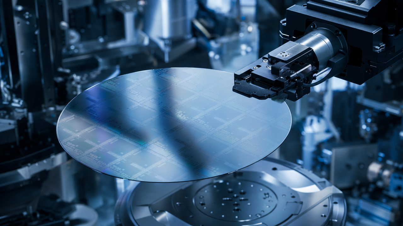
In June 2026, inside SMIC's 12-inch wafer fab in Lingang, Shanghai, a 300mm silicon wafer glided across the work stage of an ASML NXT:2050i — the most advanced immersion DUV lithography machine that is not EUV. Exposure, development, etching, thin-film deposition, polishing, repeated dozens of times. Between each step, the wafer traveled along kilometers of internal transport lines. After more than 400 process steps, it was finally diced into hundreds of chips. SMIC, the parent company of this fab, posted 67.323 billion yuan in revenue in 2025, up 16.5% year-on-year, with net profit of 5.041 billion yuan, up 36.3%. The company produced 10.1263 million wafers in 2025, with monthly capacity exceeding 1 million 8-inch equivalents and a utilization rate of 93.5%.
At the same time, at Hua Hong's Baoshan fab complex, the 12,000-wafer-per-month FAB9 line was ramping toward its 2026 target of 83,000 wafers per month. Hua Hong's full-year 2025 revenue was USD 2.402 billion, up 19.9%, with gross margin of 11.8%; both the 8-inch and 12-inch lines were running at full utilization, FAB9 had cumulatively processed over 100,000 wafers, and the ramp was on track.
At Nexchip's Hefei fab, downstream display driver IC orders had been booked through Q3 2026; for the first three quarters of 2025, the company posted 8.13 billion yuan in revenue, up 19.99%. At CanSemi in Guangzhou's Huangpu district, revenue rose from just over 1 billion yuan in 2023 to 2.582 billion yuan in 2025, more than tripling in three years.
This is China's wafer foundry industry as of 2025. An industry widely seen as the "summit of manufacturing" went through an unprecedented capacity expansion wave from 2024 to 2026.
But the cadence in Taipei and Seoul was different. In Q3 2025, TSMC took 72% global pure-foundry market share — 3nm contributed 24% of wafer revenue, 5nm 36%, and 7nm and below combined hit 74%. Samsung Foundry's share slipped from 8.1% to 7.7%. Mainland China's leaders combined held about 15% of global share — still an order of magnitude behind TSMC.
The mature-node expansion wave and the advanced-node breakthrough battle happened simultaneously in 2025–2026. The former is a "capacity-for-market" grind; the latter is a "single-point breakthrough" siege. This report walks across 14 chapters from industry overview, node breakdown, process barriers, key players, capacity expansion, price cycles, policy drivers, customer structure, and risk factors, all the way to future scenarios. It answers one fundamental question: now that mainland China's wafer foundries have built credible stock at 28nm and above, and made initial breakthroughs at 7nm and below, where will they be choked — and where will they break through?
To understand this question, one must first place wafer foundry within the broader semiconductor value chain. The chain stretches from design (fabless and IDM in-house design, plus EDA and IP tools) to manufacturing (foundries or IDM fabs), packaging and test, equipment (lithography, etch, deposition), and materials (wafers, photoresist, specialty gases, photomasks, sputtering targets). Manufacturing typically captures 30%–40% of the chain's total value.
Within manufacturing, the "foundry model" pioneered by TSMC founder Morris Chang in 1987 reshaped the entire industry. It separated design from manufacturing, allowing fabless companies (Apple, NVIDIA, AMD, Qualcomm, MediaTek, etc.) to flourish without owning fabs. Today, IDM and fabless+foundry each occupy roughly half of the global market — IDMs dominate memory, analog, and automotive power; fabless+foundry dominates logic, SoC, AI, and mobile communications.
Mainland China's foundry development rode the rise of the global foundry model, but on a distinctively challenging path. SMIC was founded in 2000 by David Wang with just USD 1.4 billion in initial capital — two orders of magnitude smaller than TSMC at the time. Two decades later, in 2025, SMIC's standalone revenue of USD 9.3 billion has caught up to become the world's second-largest pure-play foundry. Hua Hong evolved from the Japanese-Chinese joint venture Hua Hong NEC and specialized in specialty processes. Nexchip, CanSemi, and others are newer foundries that emerged after 2015, focusing on niche differentiation.
The rise of these foundries reflects China's "tech self-sufficiency" strategy combined with "supply chain reinforcement." From 2000 to 2015, mainland Chinese foundries followed a "gradual introduction–digestion–innovation" route. The 2018–2020 export-control escalation against Huawei and SMIC pushed the strategy to "all-out localization." The cost was high — sharp capex strain, gross margin pressure, loss of overseas customers. But the long-term reward followed: in five years, advanced nodes broke through to roughly TSMC's 2020 level; mature nodes scaled to the world's second-largest cluster; the local supply chain came into being.
Chapter 1: Industry Overview — 2025 Global and China
Wafer foundry (foundry, for short) converts a chip design company's layout into physical chips. From ingot slicing, polishing, and chemical cleaning to lithography, etching, thin-film deposition, ion implantation, CMP, thermal processing, and on to testing, dicing, and packaging — a 300mm silicon wafer goes through 400–500 process steps over two to three months. The foundry runs this marathon: it does not design chips, does not sell branded products, only converts customer layouts into finished wafers, for a processing fee. It is capital-intensive, technology-intensive, talent-intensive, and policy-sensitive. The barrier to advanced-node foundry work is so high that only a handful of companies worldwide can perform it.
Key 2025 numbers framing the global foundry industry:
Total scale: Global pure-foundry market about USD 150 billion in 2025, up 15%. Counterpoint Research's broader "Foundry 2.0" (pure-play + IDM foundry + memory foundry + OSAT) hit USD 85 billion in Q3 2025 alone, up 17% year-on-year.
Market share: TSMC 72% of Q3 2025 pure-foundry share, Samsung Foundry 7.7%, SMIC 5.9%, UMC 4.2%, GlobalFoundries 3.5%, Hua Hong 1.9%. Top six combined hold more than 95%.
Mainland China overall: Combined wafer foundry capacity exceeds 2.2 million wafers per month (8-inch equivalent) — about 1.5 million wafers per month of 12-inch and about 700,000 of 8-inch. Total industry revenue reached about 200 billion yuan in 2025, up about 15%. Mainland China's top twelve foundries combined hold over 15% global share, nearly three times the 2018 level.
Utilization: Mainland China foundries averaged above 85% in 2025; leaders ran above 93%. The 8-inch lines were especially tight — fully utilized at most leaders. A sharp turn from 2023, when SMIC utilization briefly fell below 70% in the industry-wide inventory correction.
Capex: Mainland China foundries spent about USD 13 billion combined in 2025, down ~10% but still historically high. SMIC alone spent over USD 7 billion — more than half the industry total. The 2026 guidance is roughly flat, meaning Chinese foundries will keep investing over 100 billion yuan annually.
Advanced-node share: Mainland China foundries' revenue mix remains dominated (about 90%) by 28nm-and-above mature nodes; advanced nodes (14nm and below) are under 10%. The opposite of TSMC, where 7nm and below took 74% of wafer revenue in Q4 2025 (3nm 24%, 5nm 36%, 7nm 14%).
Downstream applications: Consumer electronics, display driver ICs, PMICs, automotive electronics, industrial control, IoT — these dominate mainland China foundries' end markets, all centered on 28nm–110nm mature nodes, where the demand is for yield, stability, and cost-effectiveness rather than process leadership.
Global landscape: The pure-foundry duopoly is unshaken. TSMC dominates almost all advanced-node share; Samsung Foundry barely holds the No. 2 position at 3nm and below. Mainland Chinese foundries lead reverse-replacement at mature nodes domestically and have just taken the first independent step at advanced nodes.
Looking at the ten-year window from 2015 to 2025: 12-inch monthly capacity grew from about 500,000 to 1.2 million wafers, CAGR ~19%; 8-inch from 550,000 to 700,000, CAGR ~5%; total revenue from 91.6 billion to nearly 200 billion yuan, CAGR ~17%. Industry-wide CAGR is well above the global average. But the price has been heavy — capex intensity far exceeding global peers (long-term above 50% of revenue, versus TSMC ~40%, UMC ~25%, GlobalFoundries ~20%), depreciation drag is severe, gross margins remain below international peers, and the EUV ceiling continues to block five-nanometer and below.
In three numerical groups for 2025 mainland China foundry: Expansion — 12-inch wafer monthly capacity up from 500k in 2020 to 1.2M in 2025, CAGR 19%. Breakthrough — five years of advanced-node breakthrough roughly matching what international peers took ten years. Gap — total volume about 20% of TSMC; advanced-node (7nm and below) capacity about one-tenth of TSMC; gross margin ~20% vs TSMC ~60%; most-advanced production node lags TSMC by 5–6 years. Expansion, breakthrough, gap — these three groups capture the real picture of 2025 mainland China foundry.
Chapter 2: Node Breakdown — Applications and Per-Wafer Value at Every Nanometer
A "node" in foundry terminology is the most discussed and most misunderstood concept in the industry. Before 2000, node names corresponded to gate length — 180nm node meant about 180nm gate. After 2000, with transistor structures evolving from planar MOSFET to FinFET to GAA, node naming detached from physical dimensions and became more a "process generation marker" or even marketing label. TSMC's "7nm" has gate lengths of about 20nm, with density approximating early 7nm targets.
Equivalent density gives a better cross-node comparison (transistors per square millimeter, MTr/mm²): 180nm ~1.2; 130nm ~2.8; 90nm ~5; 65nm ~9; 45nm ~16; 28nm ~36 (last planar MOSFET generation); 14/16nm ~51 (first FinFET); 10nm ~72; 7nm (N7) ~90 (third-gen FinFET); 7nm (N7+) ~110 (some EUV); 6nm (N6) ~145 (EUV); 5nm (N5) ~160 (EUV); 4nm (N4) ~170 (EUV); 3nm (N3) ~250 (final FinFET + EUV); 2nm (N2) ~313 (first GAA). Each generation gives a 30–50% density bump.
28nm: The mature-node "golden median." Last planar MOSFET generation and widest pre-FinFET node. Per-wafer pricing USD 3000–3500, gross margin from 20–50% depending on foundry. Covers consumer SoCs, automotive MCUs, 5G RF and baseband, AI co-processors, display drivers, PMICs, image sensors. The reason it is the "golden median": it sits at a long-term stable equilibrium of performance/power/cost/yield, with per-transistor cost still near historical lows. Global monthly demand grows from 3.6M wafers in 2023 to a projected 4.8M by 2027.
20/22nm: Same generation as 28nm; 22nm is the low-power variant.
16/14nm: FinFET first generation. Per-wafer USD 4800–5800. Downstream: mid-range smartphone SoCs, automotive SoCs, edge AI inference, crypto compute (early Bitcoin miners), networking. SMIC mass-produced 14nm FinFET in 2020 — first mainland Chinese foundry to do so.
7nm and N+1/N+2/N+3: FinFET limit generation. TSMC's N7/N7+/N6/N5/N4 all moved to EUV. SMIC, locked out of EUV, paved its own path with DUV multi-patterning — internally coded N+1/N+2/N+3. TechInsights teardowns of Huawei Kirin chips show: 9000S → N+2, 9020 → N+2 improved, 9030 → N+3. Yields: N+2 estimated 20–40%; N+3 still climbing. Per-wafer cost likely USD 8,000–11,000 — higher than EUV 7nm after correcting for low yield.
5nm: EUV mainstream. TSMC N5/N5P/N4/N4P pricing about USD 14,000–16,000 per wafer. SMIC has launched 5nm pilot runs, with regular production targeted for 2026–2027 — still on DUV multi-patterning.
3nm: GAA entry. TSMC N3 still uses FinFET; Samsung 3GAE leads with GAA. TSMC per-wafer over USD 20,000 — locked into Apple/NVIDIA/AMD/Qualcomm/MediaTek orders through H2 2026.
2nm and 1.4nm: GAA mainstream. TSMC N2 ramps in H2 2025–2026; Samsung 2GAE in parallel. SMIC has not announced a public roadmap for this generation.
Per-wafer price gradient — 28nm USD 3,500 → 20nm USD 4,000 → 14nm USD 5,500 → 7nm EUV USD 8,000 / DUV multi-patterning USD 10,000 → 5nm USD 15,000 → 3nm USD 20,000. Doubles per node, but chip count per wafer doesn't scale; mask cost, R&D, and equipment depreciation all rise. The per-transistor cost may actually inverse.
This asymmetry is the key to understanding the foundry business. 28nm is the "most economical" node — hence the largest global demand. Advanced nodes carry premium per-wafer value but are locked into Apple/NVIDIA/AMD/Qualcomm/MediaTek — about a dozen top fabless customers. Middle nodes get squeezed from both ends.
Per-wafer cost decomposition: depreciation 30–40%, materials 20–25%, labor 10–15%, energy 5–8%, sub-contracting 5–10%, R&D amortization 5–10%. Materials at the 28nm node: silicon wafer USD 120–150, specialty gases USD 50–80, photoresist USD 20–40, photomask amortization USD 80–120, CMP slurries USD 10–20, sputtering targets USD 10–20, cleaners USD 10–15, etchants USD 10–15, others USD 20–30 — totaling USD 350–500 per wafer at 28nm; about USD 1,000–1,500 at 5nm/3nm.
Mask cost is the most extreme cost item. 28nm: USD 1.5–2M per mask set; 14nm USD 3–4.5M; 7nm USD 8–12M; 5nm USD 12–18M; 3nm USD 20M+. Masks amortize across wafer volume — if a chip's lifetime volume is 100,000 wafers, per-wafer mask cost is USD 20–300, depending on node. That's why advanced nodes only work for super-high-volume flagship chips; custom ASICs cannot bear mask cost.
Equipment depreciation is similarly underappreciated. An EUV lithography machine (NXE:3800E) costs EUR 180–200M, depreciated over 8 years gives EUR 22–25M annually. At 10,000 wafers per month, single-machine EUV depreciation per wafer is USD 180–200 — but a 100k-wafer 5nm line needs 10–12 EUV machines, totaling USD 2,000–2,500 per wafer just in EUV depreciation.
By node — different foundries have very different cost curves. TSMC's 28nm and 5nm have run for years with depreciation largely paid down; cash cost is relatively low. SMIC's 28nm has reached steady state but 14nm and N+2/N+3 remain in depreciation; cash cost is higher. This is fundamentally why TSMC's gross margin is well above SMIC's.
A node's market life is typically 15–20 years. 28nm has been mainstream since 2011 and remains so. 40nm since 2009 still has active capacity. 65/90/110/130nm capacity introduced 20+ years ago is still producing. From a node-life perspective, mainland China's 2020–2025 expansion in 28/40/55/90nm gives a 10–15 year runway — a long-payback but low-risk investment.
By "application density" (average chip demand per node), 28nm spans almost every end-market segment and has the highest demand tolerance. 14nm requires more customer concentration. 3nm has only a dozen customers — extreme concentration risk; a single flagship cutoff can leave a fab idle.
By foundry differentiation, TSMC covers all nodes (50um to 2nm) with margins concentrated at 7nm and below (74%); Samsung Foundry covers from 90nm down, focused on 5nm and below; UMC exited below 20nm, focused on 28/22/14nm; GlobalFoundries exited below 14nm; SMIC covers from 50um to N+3 (advanced under DUV multi-patterning constraint); Hua Hong covers 90–350nm with specialty processes; Nexchip leads display drivers at 40/55/90/150nm; CanSemi focuses on pure analog at 65/90/180nm.
Understanding the node-value-application-life four-dimensional asymmetry helps explain mainland China's "stabilize mature nodes first, climb advanced nodes next" strategy. It is gradient-by-economics+customer density+capacity absorption — not a "single-leap to bleeding edge" gamble.
Chapter 3: Process Barriers — DUV to EUV, FinFET to GAA, Wafer to Advanced Packaging
A wafer's path from raw silicon to finished die runs through hundreds of process steps. Roughly divided into Front-End-of-Line (FEOL — diffusion, implantation, gate formation), Middle-of-Line (MOL — contacts, local interconnect), and Back-End-of-Line (BEOL — metal interconnect).
FEOL is the hardest and most expensive. At 28nm: 60% of total process steps and 70% of equipment investment. At 7nm: 70% of steps, 80% of equipment investment. Its core is lithography, etch, and deposition — all requiring nanometer precision.
The most expensive single piece of equipment is the lithography machine. An ASML EUV NXE:3800E costs EUR 180–200M; next-gen High-NA EXE:5000 hits EUR 350M. The core difficulty is the light source — EUV uses 13.5nm extreme-ultraviolet light generated by hitting a tin droplet with a high-power CO2 laser; the resulting plasma radiates EUV with under 1% energy-conversion efficiency. ASML and Cymer spent nearly 20 years engineering this. Only ASML currently can make EUV lithography globally; DUV immersion is dominated by ASML (Nikon and Canon have minimal share). Mainland China's most advanced lithography machine is Shanghai Micro Electronics' 90nm SSA600; whether it can support 28nm and below mass production remains under verification. This is the deepest choke point.
Export controls: ASML stopped EUV shipments to mainland China in 2020. In September 2023, the Netherlands extended an export license requirement to NXT:2050i and NXT:2100i (high-end DUV immersion). Service support to existing equipment is increasingly restricted from 2024 onward.
Transistor structures: 28nm planar MOSFET → 14/16nm FinFET → 3nm GAA. Each generation brings exponential process step growth. FinFET's core difficulty is fin geometry — taller and narrower fin gives more current per area but harder process control. GAA stacks horizontally several "nanosheets," further multiplying process steps. SMIC's most advanced structure remains FinFET (N+2/N+3); GAA roadmap not yet public.
Process step counts: 28nm planar MOSFET ~400–450; 14nm FinFET ~500–600; 7nm EUV ~1000; 5nm EUV ~1100; 3nm FinFET ~1300; 3nm GAA ~1500. Each extra step adds equipment time, yield risk, and cost.
Advanced packaging: With front-end blocked, back-end packaging becomes the new battleground. TSMC's CoWoS, SoIC, and 3DFabric serve as "patches" and "extensions" for advanced nodes. TSMC's CoWoS monthly capacity expands from 20k in 2024 to over 80k in 2026 — almost entirely locked into NVIDIA, AMD, and Broadcom AI accelerator orders. Mainland China's ChangElectric (JCET), TFME, HuaTian, and Crown Tech are ramping 2.5D/3D packaging; SMIC's SJ-Semi handles bumping and RDL; Hua Hong is building silicon photonics, embedded memory, and IGBT integration.
Yield: Beyond paper specs, yield is the real moat. TSMC's 3nm has stabilized above 80%; SMIC's 14nm climbed from under 30% in 2020 to over 90% by 2024; SMIC's 28nm from 75% in 2020 to 92% by 2024. Yield improvement requires the "learning curve" — each wafer's data feeds process optimization, needing time, customer orders, equipment stability, and team continuity.
Specialty processes: Beyond mainstream logic, BCD (bipolar-CMOS-DMOS), embedded NVM (eFlash/eMRAM), ultra-high-voltage, ultra-low-power, analog/RF, CIS, power devices (IGBT/SiC/GaN) form the "specialty process" track. Hua Hong leads in mainland China, with BCD covering 55–90nm; IGBT, super-junction MOSFET, and SiC platforms keep iterating. SMIC, Nexchip, and CanSemi all have differentiated specialty platforms.
The essence of the process barrier is engineering trade-off between "advancement × economics × reliability." Mainland China's strategy: push mature nodes to the limit within the equipment they can access, deepen specialty platforms, force-march advanced nodes via DUV multi-patterning. The path is high-cost, low-yield — but every step forward buys one more increment of self-sufficiency.
Equipment-supply detail: A 12-inch line includes lithography (immersion DUV/EUV), etch (dry/wet, plasma), thin-film deposition (CVD/PVD/ALD), CMP, ion implantation, thermal processing (RTP/diffusion), metrology (CD, defect inspection, thickness, electrical), wet cleaning, EBL, wafer handling. A 100k-wafer 12-inch line costs USD 6–8 billion in equipment — lithography 30%, etch 15%, deposition 15%, metrology 10%, CMP/clean 8%, implantation 5%, other 15%.
Lithography setup specifics: At 28nm, ~8–12 ASML NXT:1980i (each ~4500 wpm), 2–3 DUV critical-layer exposures; at 14nm FinFET, 5–8 each of NXT:2000i and NXT:2050i, 5–7 critical layers; at 7nm EUV, TSMC uses NXE:3400B/3600D (each ~3000 wpm), 8–10 critical EUV layers; SMIC, lacking EUV, uses NXT:2050i and NXT:2100i for multi-patterning, 12–16 critical layers — double the steps.
Etch and other equipment localization: AMEC's ICP and CCP plasma etchers are in mass production at SMIC, Hua Hong, and YMTC at 28nm and 5nm memory nodes. NAURA covers silicon, oxide, and metal etch up through advanced. Mainland China etch localization reached ~60% by end-2025. Deposition localization ~55%, CMP ~40%, cleaning ~50%, metrology under 25%, ion implantation ~30%, EBL and EUV source still in lab research.
China's localization path: middle-to-back end first, front-end follows, metrology gap fills last. Local equipment can cover ~60–70% of the 400–500 process steps — concentrated in deposition, etch, cleaning, CMP. Lithography, metrology, and key inspection remain the gaps.
Lithography is the deepest of the three-doors (process barrier, equipment barrier, materials barrier). EUV's engineering challenge is single-source (Cymer/ASML's LPP), 13.5nm wavelength, light source at 250W average power, conversion efficiency under 1%. Optical system: EUV light has extreme low reflectance, requiring reflective (not transmissive) optics; mirrors with surface roughness under 50 picometers (Zeiss). Mechanical: wafer stages and mask stages running at meters per second with sub-nanometer positioning. Vacuum: 10^-5 Pa requires a dozen vacuum pumps in tight coordination. Integration: tens of thousands of parts, hundreds of thousands of hours of engineering iteration. Why ASML alone makes EUV — this is a "full-chain integration + engineering experience + customer validation + sustained capital" multi-barrier stack.
China's EUV roadmap: light source (LPP/DPP/SXR parallel), optics (design + coatings), mechanical (precision motion), vacuum, integration — Shanghai Micro Electronics, CAS Institute of Optics & Mechanics, Huazhuo Precision, Fuguang Optics co-developing. Predicted first prototype "light-up" by 2029–2030; pre-production by 2032–2033; mass-production-ready unit by 2035–2036.
DUV immersion localization: SMEE's SSA600 (90nm) is in service; SSB800 (28nm) is roadmapped. Compared to ASML NXT:1980i/2000i/2050i, throughput, alignment, stability lag. Expected 28nm DUV mass-production verification by 2027–2028; 14nm by 2030.
Photoresist coupling: Even with domestic EUV in 2030, EUV photoresist localization may not arrive until 2035+ — Japan's JSR, TOK, Sumitomo, Shin-Etsu still dominate.
Chapter 4: Key Players — Mainland China vs International Comparison
Foundry classification first. By business model: pure-play foundry (TSMC, SMIC, Hua Hong, UMC, etc.) vs. IDM foundry business (Samsung Foundry, Intel Foundry Services). By process scope: all-node (TSMC, SMIC), specialty (UMC, Nexchip), specialty-process (Hua Hong, CanSemi, Tower, X-FAB). By capacity scale: tier-1 (100k+ wpm 12-inch), tier-2 (50–100k), tier-3 (20–50k), tier-4 (under 20k). In China: SMIC and Hua Hong are tier-1; Nexchip and CanSemi are tier-2; ShangAJ, XMC, Pingtouge JV are tier-3.
SMIC: Mainland China's foundry leader. 2025 revenue 67.323 billion yuan (up 16.5%); net income 5.041 billion (up 36.3%); ex-recurring 4.124 billion (up 55.9%); gross margin 21.6%. Produced 10.1263 million wafers in 2025; monthly capacity > 1M 8-inch equivalent, including ~600k 12-inch and ~400k 8-inch. Process: 50um to 7nm, focused on 28nm, 40/55nm, 110/130nm, 14nm FinFET, with leading edge at N+1/N+2/N+3. Customer mix: HiSilicon, UNISOC, Will Semi, GigaDevice, Goodix, ZTE Microelectronics, SmartSens. Overseas share dropped from 50% in 2020 to under 25% in 2025 — mostly Broadcom, Qualcomm, ON Semi residuals. SMIC has 12-inch fabs in Shanghai, Beijing, Shenzhen, and Tianjin; the new Lingang, Jing-Cheng, and Shenzhen-New fabs are the 28nm-and-below expansion battlegrounds. 2026 capex guidance flat to 2025 — still over USD 7 billion.
Hua Hong: Specialty-process leader. 2025 revenue USD 2.402 billion (up 19.9%); gross margin 11.8%; net loss narrowing. 8-inch monthly capacity 180k (Wuxi + Shanghai); 12-inch reaching 83k per month at FAB9 by 2026. Process: 90nm to 350nm specialty, leading BCD power management, embedded eFlash NVM, IGBT and super-junction MOSFET, CIS, MCU. Customers: Silan, Yangjie, CR Micro, UNISOC, Fuman, Sichuan Huicong, etc. FAB9 (Wuxi 12-inch) targets monthly capacity 120k.
Nexchip: Hefei's largest foundry. First three quarters of 2025 revenue 8.13 billion yuan, up 19.99%. 12-inch monthly capacity 125k, all in Hefei. Process: 150 to 28nm, leading DDIC (display driver), CIS, PMIC, MCU specialty. Global DDIC share ~15%, domestic ~70%. Customers: Himax, Novatek, JD Microtech, FocalTech, etc.
CanSemi: Guangzhou pure-analog foundry. 2023/2024/2025 revenue: 1.044, 1.681, 2.582 billion yuan — triple in three years. End-2025 12-inch monthly capacity 63,300; 2026 planning to 125k. Process: 90–180nm specialty analog/power. Customers: Joulwatt, NovoSense, Chipown, Halo Micro, Marvell-Power, LCEM, BiyiMicro, etc. December 2025 launched IPO filing for ~7.5 billion yuan, valuation over 25 billion yuan.
Hefei Changxin (CXMT): Not strictly a foundry; mainland China's DRAM IDM. 2025 17/19nm DDR5/DDR4 production at ~200k 12-inch wafers per month. Process node from 19nm in 2020 to 17nm in 2025; products from DDR4 to DDR5, LPDDR5, HBM3. 2026 capacity planning ~250k.
Others: Shanghai Active-Semi (积塔), Wuhan XMC, CR Micro, Silan Jike, Changxin JC, Shaoxing SilicC, Changsha BYD Semi — ~15 mid-size or specialty foundries, combined ~800k wafers per month 8-inch equivalent.
International comparison: TSMC: pure-foundry leader. Cumulative first 11 months 2025 revenue NT$3.47 trillion (+32.8%); full-year ~USD 105 billion. Q3 2025 share 72%. 3nm 24%, 5nm 36%, 7nm 14%, 7nm and below 74%. Core moat: advanced-node monopoly + customer lock-in (Apple, NVIDIA, AMD, Qualcomm, MediaTek, Broadcom, Amazon, Google).
Samsung Foundry: 7.7% Q1 2025 share, slipping. 3nm GAA yield trails TSMC; 5/4nm orders flowing away. Strategy: catch TSMC overflow + secondary supplier to NVIDIA, Qualcomm, AMD.
GlobalFoundries: Q3 2025 share 3.5%. Exited below 14nm, focused on 12nm and above specialty. CHIPS Act gives ~USD 1.57B and DoD ~USD 3.1B contract. Downstream: auto, industrial, AIoT, 5G RF, PMIC.
UMC: Q3 2025 share 4.2%. Exited below 20nm. Core in 28/22/14nm. 2025 announced Intel JV for 22nm FinFET in Arizona — direct competition to mainland China.
VIS + PSMC: Taiwan mid-size, combined ~2.5% share. VIS in 8-inch power/analog; PSMC in memory foundry + display driver.
Tower + X-FAB: Israeli and German specialty foundries, smaller but deep. Compete directly with Hua Hong and CanSemi in SiGe, RF SOI, CIS, MEMS.
Horizontal comparison: SMIC revenue has surpassed GlobalFoundries (USD 7.6B 2025), is close to UMC (USD 9.0B), but gross margin is still lower — SMIC 21.6%, UMC ~30%, GF ~25%, TSMC ~58%. The margin gap reflects process mix: TSMC's high margin comes from 3/5/7nm; UMC's from steady-state 22/28/40nm; SMIC's is held down by advanced-node depreciation drag.
Mainland China's position: tier-2 by volume, behind TSMC and Samsung; process mix concentrated on mature nodes plus a slice of advanced; customer mix overwhelmingly domestic; gross margin still in expansion-phase compression.
Differentiation by foundry in 2026: SMIC: "comprehensive logic foundry," focused on 28/14nm + N+2/N+3. Logic SoC/MCU/AI compute ~65%, analog/power ~15%, CIS/MEMS ~10%, other 10%. Hua Hong: "specialty process," 5 BCD nodes from 55nm to 180nm, 2500+ IP. eFlash for automotive MCU and IoT. IGBT/super-junction MOSFET for EV main drives and solar inverters. CIS for smartphones, security, automotive. Nexchip: "display driver specialist," global #1 single-niche share. DDIC sells $1–1.5 each but ships 6+ billion units annually. CanSemi: "pure analog foundry," post-2020 specialty platform — BCD, ultra-high-voltage, embedded NVM, CIS, MCU. Domestic fabless lineup of "small-but-strong" analog IC designers.
This multi-tier differentiation in mainland China — leader SMIC + specialty Hua Hong + Nexchip/CanSemi specialists + CXMT memory + multiple niche foundries — avoids cannibalistic competition and entered a "niche-differentiation healthy expansion" stage.
Chapter 5: Mainland China 12-Inch / 8-Inch Capacity Breakdown — 2025–2027
To grasp the expansion map, the 12-inch vs 8-inch difference matters. A 300mm 12-inch wafer has 707 cm² effective area, 2.25x more chips than an 8-inch (200mm). 12-inch wafer cost is 2–3x of 8-inch, but per-chip cost is 30–50% lower. That's why 12-inch is mainstream. But 8-inch is not retired — for power devices (IGBT, MOSFET, diodes), analog ICs, sensors, MEMS, 8-inch remains primary. Reasons: 8-inch depreciation is paid off; new 8-inch is actually more expensive than 12-inch in some cases; certain specialty processes are more mature at 8-inch; customers value process continuity. China is the world's largest 8-inch capacity base — Hua Hong (Wuxi + Shanghai), SMIC (Beijing, Shanghai, Shenzhen), CR Micro, Silan, BYD Semi, Changsha BYD, Yandong — totaling ~700k wafers per month, ~30% of global 8-inch.
12-inch capacity by foundry as of June 2026: SMIC: SN1+SN2 in Lingang ~120k 12-inch monthly (planning 160k by 2026); Jing-Cheng (Beijing) ~100k (planning 150k); Shenzhen ~50k; Shanghai legacy ~60k; Tianjin in planning. Total ~600k by 2026 plan, 750k+ by 2027.
Hua Hong: Shanghai 12-inch (separated from Hua Hong Grace 8-inch); Wuxi FAB7 12-inch (90/65/40nm specialty, 120k); FAB9 (55/40nm and below, 83k by 2026 plan, 120k long-term). Total 12-inch ~200k by 2026, 300k+ by 2027.
Nexchip: Hefei Fab1/2/3 (150/110/90/70/55/40/28nm specialty), 125k 12-inch; 140k by 2026.
CanSemi: Guangzhou Fab1/2/3/4 (90/65/55nm specialty), 63.3k 12-inch; 125k by 2026.
Hefei Changxin (CXMT): Hefei 12-inch memory fab (17/19nm DDR5/DDR4), ~200k 12-inch (memory, not foundry).
Shaoxing SilicC: 8+12-inch combined, 100k 8-inch equivalent.
Wuhan XMC: NOR Flash + CIS foundry, 60k 12-inch.
Shanghai Active-Semi (积塔): Specialty (auto MCU, power devices, CIS), 50k 12-inch; planning 80k by 2026.
Changxin JC: Hefei (separate from CXMT) NOR/MCU specialty, 30k 12-inch.
Total mainland China 12-inch foundry (excluding memory and IDM): ~1.2M wpm by end-2025, ~1.5M by 2026, ~1.8M by 2027.
By node split (foundry, ex-memory): 28nm and below ~200k wpm; 40/55nm ~300k; 90/110/130nm ~400k; 180nm+ ~300k.
Geographic clusters: Shanghai cluster (Zhangjiang-Lingang-Songjiang): SMIC SN1/SN2, SMIC legacy, Hua Hong Grace, total ~350k 12-inch + 120k 8-inch. Hefei cluster (Jingkai-Gaoxin): Nexchip Fab1/2/3, CXMT, Changxin JC, TFME packaging, NAURA Hefei — total foundry+memory ~320k 12-inch. Guangzhou cluster (Huangpu): CanSemi Fab1/2/3/4, Lianhe Semi — ~60k 12-inch; planning 125k by 2026. Beijing cluster (Yizhuang): SMIC Jing-Cheng, Yandong, JC Mips, NAURA HQ — ~150k 12-inch + 80k 8-inch. Shenzhen cluster (Nanshan): SMIC Shenzhen, BYD Semi, Guowei — ~60k 12-inch. Wuxi-Suzhou cluster: Hua Hong Wuxi FAB7/FAB9, JCET, Zhonghuan wafer, Yituang — most complete regional ecosystem in mainland China.
Ramp timelines: A new 12-inch line: foundation to first wafer 18–24 months; first wafer to steady state (80%+ of design capacity) another 12–18 months; full "zero to steady state" cycle 30–42 months. Equipment lead time for ASML DUV: 24–36 months; EUV 36–48 months. Single critical equipment "order to mass production" can stretch to 42–60 months. Yield ramp: 28nm planar MOSFET 12–24 months (from 50% to 90%); 14nm FinFET ~36 months; N+2/N+3 type ~60 months. The 2026–2028 capacity coming online today was committed to in 2022–2024; the 2029–2030 capacity depends on 2025–2026 commits. So the next five years' capacity footprint is essentially locked.
Chapter 6: Advanced Process Breakthrough — N+1/N+2/N+3 and 14nm Actual Yield
Mainland China's advanced-process breakthrough is essentially SMIC alone.
Timeline: 2018 14nm FinFET launch → 2019 production, initial ~30% yield; 2020 ~50%; 2021 75%; 2022 85%; 2023 90%; 2024 90%+. Five years from launch to stable.
N+1: 14nm + DUV multi-patterning (SAQP/SADP), pitch ~36nm, mid-pack near early TSMC N7. Lab-deconstructed in 2021–2022 but not in volume.
N+2: Pitch ~32nm, density ~90 MTr/mm² — comparable to TSMC N7. TechInsights confirmed Kirin 9000S (2023) used N+2. This was the milestone of mainland China crossing the 7nm threshold.
N+3: Further density improvement, pitch ~28nm, density ~140 MTr/mm² — between TSMC N6 and N5 early. Still FinFET, still DUV multi-patterning. The Kirin 9030 (Mate 80 flagship) and Huawei Ascend 910C/920 use N+3.
Yield: N+2 estimated 20–40%, N+3 still in 20–30% range. Single-chip viable yield is 1/3–1/2 of TSMC same-generation. Effective cost is double or more.
Capacity: End-2025 SMIC 7nm-and-below combined ~45k wpm; 2026 plan 60k; 2027 80k.
5nm route: Confirmed in pilot per 2025 H1 report; expected limited production 2026, ramp 2027–2028. Still DUV multi-patterning, 3–4 patterning steps, 33% more process steps than 7nm; yield challenge greater.
Applications: N+2/N+3 currently serves Huawei Kirin SoCs, Huawei Ascend AI accelerators, and Hygon DCU. Ascend 910C 2026 target output ~300k units, actual delivery may be ~60% of target due to yield drag (SemiAnalysis).
Equipment dependency: DUV multi-patterning depends heavily on equipment reliability, etch uniformity, deposition uniformity, metrology precision. Local equipment (NAURA, AMEC, YITUANG, ACM, HCSC, KingSemi) has broken through at 28/14nm; 7nm-and-below verification still ongoing.
Breakthrough cadence: 2020 → 2025 from 14nm to N+2/N+3 steady state — five to six years of advanced process attack. Next five years (2026–2030) expected: 5nm DUV multi-patterning production, GAA structure trial, domestic EUV source/lithography engineering verification, advanced packaging (CoWoS-like) capacity ramp.
Gap: 5–6 years behind TSMC by node; 1/10 of TSMC in advanced-node volume; yield 1/3 to 1/2 of TSMC same-generation.
Cross-generation TechInsights detail: Kirin 9000s (2023): SMIC N+2, MMP ~28–30nm, ~90 MTr/mm², matching TSMC N7. Kirin 9020 (2024): N+2 refinement, ~110 MTr/mm², matching TSMC N7+. Kirin 9030 (2026): SMIC N+3, MMP ~25–26nm, ~140 MTr/mm², between TSMC N6 and N5 early.
So mainland China's most advanced node N+3 = TSMC N6–N5 early ≈ 5–6 year node lag, achieved with doubled process steps via DUV multi-patterning.
Next-generation 5nm target: still FinFET + DUV multi-patterning, MMP ~20nm, ~180 MTr/mm² — matching TSMC N5/N5P (2020–2021). Predicted: limited production H2 2026 to 2027; ramp 2027–2028.
Post-5nm: 3nm and below force GAA. SMIC has no public GAA roadmap, but supply-chain trace shows R&D underway.
EUV absence consequences: Below 3nm, EUV is effectively required. TSMC N3 critical-layer EUV ~20 layers; GAA N2 ~25 layers. DUV multi-patterning at those nodes triples or quadruples process steps — yield and cost become uncontrollable. Until EUV localization, mainland China cannot truly enter 3nm GAA.
Process-engineer headcount: Each new node node requires double — TSMC's 5000-engineer node R&D team; SMIC's same-equivalent team ~1000–1500.
Yield optimization curve: From initial 30% to steady 90% takes 3–5 years. Each defect identified → fixed → optimized iterates. SMIC's 14nm curve is the typical example: 2019 mass production 30%; 2021 75%; 2023 85%; 2025 90%+. N+2/N+3 curve will be longer.
Chapter 7: Filter Factories by Process — Supply-Chain View
At chapter 7, switch perspective. The previous chapters focused on foundries themselves — revenue, capacity, nodes, yield, customers. But a foundry is not an island. Behind one fab stands a vast collaboration chain across photomasks, equipment, specialty gases, ultrapure water, photoresist, sputtering targets, CMP slurries/pads, chemicals, wafer manufacturing, and packaging — each link has hundreds to thousands of supplier factories.
From the panoramic view, one 12-inch foundry typically draws on ~800–1000 local suppliers. Photomask suppliers ~12; specialty gas suppliers ~25; photoresist suppliers ~12; ultrapure water ~5; chemicals ~50; sputtering targets ~12; CMP slurry and pad suppliers ~12; front-end equipment ~50; back-end equipment ~50; parts and consumables suppliers hundreds; test and packaging ~50.
Every supplier on this chain is an "infrastructure engineer" for mainland China's foundry ecosystem. When a foundry's sales, procurement, or process engineer needs to filter suppliers by process node, by region, by category, generic business-registry databases pull in too many non-factory entities — trading firms, consultancies, design centers — making it hard to lock in real factory leads.
「Tianxia Gongchang」 (天下工厂) is one such tool. It is a B2B sales-lead-oriented factory search platform covering 4.8 million in-production factories in China, distinct from generic "everyone gets a record" registry databases — the platform identifies factory-entity status via three mechanisms: business registry data + administrative-license data + on-the-ground cross-verification. So on the question "is this really a factory," the platform's precision substantially exceeds generic business tools.
For wafer foundry value chain, a sales engineer might ask:
Photomask supply: How many mainland China factories can produce 28nm-and-above photomasks? Which provinces? Monthly capacity? On the platform, with "photomask + semiconductor + Jiangsu/Guangdong/Hubei" as compound keywords, one can pull a full mask-supplier list — Xinshuo Semi, Aibo Semi, Disi Microelectronics, Longtu, Qingyi Optoelectronics, Luwei, etc.
Specialty gases: Wafer foundry depends on ultra-high-purity gases (NF3, SF6, WF6, SiH4, PH3, BF3, Cl2, HBr). Core suppliers cluster in Jiangsu, Zhejiang, Guangdong — Huate Gas, Yake Tech, Jinhong Gas, Heyuan Gas, Kaimeite Gas. Filter "electronic specialty gas + semiconductor + Jiangsu/Zhejiang/Guangdong" on the platform for a county-level list.
Photoresist: ArF/i-line/EUV photoresist is the deepest choke. Mainland China's catch-up players: Tongcheng Newmaterial (Qiangzi, parent of Beijing Kehua), Crystal Clear, Nanda Photoelectric, Beijing Kehua, Shanghai Xinyang. Production processes cover 28nm KrF and limited ArF. Filter "photoresist + electronics-grade + Shanghai/Jiangsu/Beijing".
CMP slurry and sputtering targets: Anji Microelectronics leads CMP slurry, Huaxue Microelectronics second; sputtering target leaders are Jiangfeng Electronics, Youyan New Material, Longhua Tech, AShi Chuang. Filter "semiconductor + slurry/pad" and "semiconductor + sputter target".
Packaging and testing: JCET, TFME, HuaTian, Crown Tech (Crown Tech for CIS), King Yuan, CR Anson, UNIC Marshal, Intel Dalian. Filter "IC + packaging/test" to find 500+ packaging-related factories nationwide.
CIS/MEMS/Discrete: Image sensor, MEMS, discrete-device factories spread across provinces. Filter by category + region for the regional supplier pool.
For a foundry sales engineer or a process-tool SaaS sales engineer who needs to pull "the Yangtze River Delta's 28nm photomask supply pool" or "the country's electronic-grade photoresist factories," generic business-registry databases pull lots of non-factory noise. The platform's differentiation: factory-entity status is its primary filter, so the resulting list "really makes things" at a substantially higher rate than generic tools.
Around wafer foundry and IC foundry as core categories, further breakdowns lead to semiconductor wafer, wafer manufacturing, IC design, semiconductor design.
Equipment and material categories: semiconductor equipment, semiconductor materials, lithography machine, etching machine, photoresist, electronic specialty gas, semiconductor specialty gas, ultra-high-purity gas, photomask, semiconductor sputter target, CMP slurry, chemical mechanical polishing, semiconductor cleaning, silicon wafer, epitaxial wafer, compound semiconductor, third-generation semiconductor.
Testing and packaging: semiconductor test, semiconductor packaging, IC packaging, advanced packaging, wafer-level packaging, wafer dicing.
Downstream device categories: power semiconductor, power device, IGBT, image sensor, AI chip, automotive chip, vehicle-mounted chip, memory chip, MEMS sensor, MEMS.
From the value-chain perspective, mainland China's wafer foundry rise is not the victory of a few foundries alone — it is the synchronized advancement of the whole chain.
Chapter 8: Mature-Node Price War — 28nm Decline from 2024 to 2026
From Q4 2023, mature-node prices declined visibly. The drivers: global consumer-electronics weakness + mainland China foundries concentrated expansion + overseas foundries (UMC, GF, PSMC) reverse-pricing to grab share.
Price curve: Q3 2023: 28nm USD 3200–3500 per wafer; 40nm USD 2800–3100; 55/65nm USD 2500–2800. Q1 2024: 28nm fell to USD 2900–3200; 40nm to USD 2500–2800; 55/65nm to USD 2200–2500. Q3 2024: 28nm steadied at USD 2800–3000; 40nm at USD 2400–2700. Q2 2025: With AI co-processors, automotive, display drivers, 5G RF rebound, prices rebounded from the bottom — still below 2023 high. H1 2026: 28nm rebounded to USD 3000–3200; 40nm USD 2600–2900. Mainland China foundries "steady pricing, no price-cut grabs" — price war is winding down.
The essence: 28nm global demand truly grew (from 3.6M wpm in 2023 to projected 4.8M by 2027), but mainland China's 28nm capacity simultaneously grew from 100k wpm in 2023 to 200k by 2025 and 350k planned by 2027. Overseas foundries (UMC, GF, PSMC) added capacity or cut prices in response. Structural surplus emerged.
Gross margin impact: SMIC Q4 2023 fell from 38% in 2022 to 16%; recovered to 18–20% through 2024; 21.6% in 2025. Hua Hong Q4 2023 fell from 35% in 2022 to under 10%; recovered to 10% in 2024; 11.8% in 2025. The shock was significant but temporary.
Overseas counter-attack: UMC + Intel announced 22nm FinFET JV in Arizona — direct competition. GF received CHIPS Act ~USD 1.57B and DoD ~USD 3.1B contract. PSMC, VIS also launched expansion. All major global foundries preparing for the next round of 28/22nm expansion.
Mainland China response: SMIC, Hua Hong, Nexchip in 2025 adopted "price floor + capacity ramp + shift toward auto/industrial/AIoT" combination. Auto/industrial customers have lower price sensitivity than consumer-electronics customers and value long-term stable supply more — they became the price-war buffer. By H2 2025, auto/industrial revenue share at all four leaders rose significantly. CanSemi crossed 40%.
Price war + expansion wave is the core contradiction. By H1 2026 it's basically reaching closure — Chinese foundries near cost floor with limited downside; overseas counter-attack constrained by capex intensity; ramp-completion drives steady-state absorption. Next wave: 2028–2029, when UMC/Intel/GF U.S. new 22nm comes online.
Foundry cost-pass-through to downstream IC designers: A 28nm mid-tier handset SoC sells for USD 12–16, of which foundry cost USD 2.5–3 (20%), packaging USD 1 (8%), R&D amortization USD 2 (15%), SG&A USD 1 (8%), gross profit USD 5–8 (~40%). Foundry cost is ~20% — looks small but is rigid. Every 10% foundry price hike compresses fabless gross margin by 2%.
Cross-node price linkage: 28nm price drops cascade to 14/20nm; also reverse-impact 40/55nm — some customers may "node-skip" toward 28nm. Foundries must manage cross-node strategies, not single-node.
Inventory cycle: Downstream fabless and brands over-stocked in 2021–2022 (chip shortage), entered destocking from H2 2022, lasted 18–24 months until H2 2024. Cycle + capacity ramp double-pressure. From 2026, inventory at normal levels; downstream entering restock — positive for foundry utilization and price elasticity.
Specialty processes "drop-resistant": BCD, eFlash, IGBT, ultra-high-voltage, CIS — pricing volatility much smaller than pure logic. Customer lock-in high. Hua Hong/Nexchip/CanSemi specialty stayed steady or even climbed during 2023–2026.
Price war's "geographic dimension": Mainland China foundries' price war is mostly domestic. Overseas customer prices remained relatively stable but volume cratered (from ~50% revenue share in 2020 to under 25% in 2025). High-margin overseas order loss + high-competition domestic order influx was the other reason for sustained margin pressure.
If next five years auto/industrial (high margin, customer-locked) and advanced-node (high per-wafer value) make progress, gross margins can recover from ~20% in 2025 to ~30% by 2030. This is the path from "price-war defense" to "margin-recovery" mode.
Chapter 9: Capex Cycle — USD 100B+ from 2024 to 2026
Foundry is the textbook capital-intensive industry — initial line investment USD 5–10B, depreciation 5–7 years. Capex cyclicity defines industry tempo.
Global cyclical pattern: Past 30 years saw five "expand-correct" cycles, each ~6–8 years. Cycle 1: 1995–2000 internet bubble. Cycle 2: 2001–2007 mobile+PC. Cycle 3: 2008–2014 smartphone. Cycle 4: 2015–2022 AI/data center/IoT. Cycle 5: 2023–2026 AI LLM + mainland China localization.
Mainland China foundry capex cycle: Sync with global but with extra localization driver.
2024–2026 mainland China foundry capex high cycle:
2024: combined USD 14B; SMIC alone USD 7.32B.
2025: combined ~USD 13B; SMIC ~USD 7B.
2026 guidance: SMIC flat (USD 7B); Hua Hong USD 1.5–1.8B; Nexchip USD 1.2–1.5B; CanSemi ~USD 1B; others ~USD 1B. Total ~USD 11.5–12.5B, down ~10%.
Absolute total 2024–2026: combined ~USD 39B (RMB 280B) — among the largest single-industry capex cycles in mainland China manufacturing history.
Equipment localization rate: 2023 under 25%, 2025 nearly 50%. Etch, deposition, CMP, cleaning lead; lithography (near 0%), metrology (25%), implantation (30%) lag.
Funding sources: Public-company operating cash (SMIC, Hua Hong), Big Fund I/II/III equity, regional industrial funds (Lingang Group, Hefei Jingkai, Guangzhou Huangpu, Shaoxing), bank loans, bonds, secondaries. Big Fund Phase III (registered capital RMB 344B) launched H2 2024. MOF RMB 60B (17.44%), CDB Finance RMB 36B, six state banks combined RMB 114B (33%).
Big Fund III investment direction: 70% equipment/material localization, 30% advanced packaging/AI memory. Foundry beneficiaries: SMIC, Hua Hong, Nexchip, CXMT, plus several new advanced-node project.
Depreciation drag: SMIC 2025 depreciation USD 2.1B (22% of revenue). Hua Hong USD 800M (33%). Short-term margin pressure, but once the 2017–2019 capex cycle's equipment depreciates out in 2024–2026, the headwind eases — entering "depreciation discharge + margin recovery" phase in 2027–2028.
International capex comparison: TSMC 2025 capex ~USD 42B (3x of all mainland China combined); Samsung Semi ~USD 35B (DRAM+NAND+Foundry); Intel ~USD 18B. Mainland China combined capex now matches Intel scale but lags TSMC by 2–3x.
Cash flow detail: SMIC 2025: operating CF ~RMB 21B; financing CF ~RMB -6B; equity raise ~RMB 10B; free cash flow ~RMB -34B (USD ~5B gap). Hua Hong 2025: operating CF ~RMB 9B; financing CF ~RMB 12B; FCF ~RMB -5B. Nexchip 2025: operating CF ~RMB 4B; financing CF ~RMB 9B; FCF ~RMB -6.5B. CanSemi 2025: operating CF ~RMB -0.5B (loss); financing CF ~RMB 8B; FCF ~RMB -9B.
Combined free cash flow gap: ~RMB 54B (USD 7.5B). Filled by Big Funds + bank loans + capital markets.
Capex's marginal return decline: 2020–2022 each capex dollar drove ~USD 1.2–1.5 revenue increment; 2023–2025 it dropped to USD 0.8–1.0. Reason: new capacity concentrated at 28/40nm (lower per-wafer value); plus 2-year ramp lag.
Capex intensity comparison: TSMC long-run capex ~30–40% of revenue. Samsung volatile. UMC/GF ~15–20%. SMIC 2022–2025 capex ~60–70% of revenue — typical "expansion-phase" mainland China.
State-level capex strategy: Big Fund I/II/III + regional funds + tax incentives + subsidies = >RMB 1 trillion firepower, "national-level financial moat." Supports expansion through short-term losses.
Equipment localization & cost: As local equipment penetrates further (~70% by 2030), per-wafer depreciation cost drops 10–15%, supporting margin recovery.
2027–2029 outlook: capex intensity drops; depreciation drag eases; localization cost reduction kicks in; gross margins recover. Classic "expansion → maturity" cycle transition.
Chapter 10: Policy Drivers — Big Fund II/III, Export Controls, Subsidies
Three policy phases: Phase 1 (2000–2013): Industry takeoff, scattered support. Phase 2 (2014–2023): Big Fund I/II + systematized support per "National IC Industry Development Outline." Phase 3 (2024–present): Localization siege via Big Fund III + regional funds + tax breaks + talent subsidies.
Each phase intensifies. Phase 1 supports single companies; Phase 2 covers key value-chain links; Phase 3 = full value chain + all nodes + all factors.
Big Fund I (2014): registered capital RMB 138.7B. Invested in SMIC, YMTC, CXMT, Sanan, Hua Hong, UNISOC. Big Fund II (2019): RMB 204.1B. Support for SMIC SN1/SN2, Hua Hong Wuxi, YMTC, CXMT, plus equipment/material/OSAT firms. Fully deployed by end-2025. Big Fund III (May 2024): RMB 344B, 15-year cycle (2024–2039). MOF, CDB Finance, six state banks co-investing. Direction: 70% equipment/material, 30% advanced packaging + AI memory. Q1 2026 cumulative deployment ~RMB 164B.
Regional industrial funds: Shanghai, Beijing, Shenzhen, Hefei, Guangzhou, Suzhou, Wuhan, Shaoxing — combined > RMB 1 trillion, larger than Big Fund III alone.
Subsidy mechanics: Direct equity (Big Fund + regional funds), tax exemptions (3-free-3-half EIT, VAT immediate refund), land discounts (free/discounted industrial land), talent bonuses (key-post personal-income-tax rebates + relocation), R&D extra deduction (R&D expense pre-tax extra deduction 100–150%), domestic equipment first-set subsidy (up to 30%), loan interest subsidies.
Export controls: US 2019 added Huawei to Entity List; 2020 SMIC; 2022 mainland China advanced foundries broadly; Netherlands Sept 2023 NXT:2050i/2100i license; Japan 2023 23-item equipment controls; Korea quietly tightened EUV photoresist + key materials.
Practical impact: Cannot buy newest EUV or new high-end DUV. Existing equipment can be used and serviced under license restrictions on parts. Strategy: accelerate domestic equipment + deeper ties with remaining overseas suppliers + cash reserves for long-term restriction.
Entity List: As of June 2026, 120+ mainland China semiconductor companies — foundries (SMIC, YMTC, CXMT, Shanghai Active-Semi), equipment makers (HCSC, YITUANG, parts of Jingsheng), designers (HiSilicon, Cambricon, Hygon, Birenetech, Suiyuan), some material vendors. Impacts vary by entity and clause.
Policy driver essence: Big Fund + regional fund + local subsidies + tax + entity-list counter-measures = "national-level financial moat." Mainland China foundry capex capability and ramp speed far exceed pure-market peers (UMC, GF, PSMC, VIS). Cost: lose subsidy support → tougher in price wars; cooperation space with overseas players keeps shrinking; advanced-node equipment/material gap needs self-breakthrough.
Global policy comparison (2022–2030 horizon, total policy investment):
Mainland China: RMB 2 trillion ($2.8 trillion USD-equivalent).
US CHIPS Act: USD 52.7B.
EU Chips Act: EUR 43B (USD 46B).
Japan: JPY 2 trillion (~USD 14B).
Korea K-Chips: ~USD 62B.
Mainland China policy intensity > all others combined ×2+. This intensity is the foundation enabling Chinese foundries to keep expanding through export-control pressure.
R&D tax credit: From 2023, mainland IC design and software extra deduction rose from 75% to 100% — directly stimulating 2023–2025 R&D spending growth.
Talent subsidies: Major regions provide tax exemption, relocation fees, child education, healthcare for key semiconductor talent. Lingang covers 1–2x personal income tax rebate; Hefei Jingkai relocation up to RMB 3M.
Land + utilities discounts: 5–8% of operating cost. Local governments offer "near-zero-cost" industrial land and discounted utilities — saving billions per fab.
Domestic equipment first-set incentives: Up to 30% subsidy. Stimulates "dare to use" domestic equipment.
Equipment import VAT refund: Effectively 13% cost reduction on imported equipment — speeds key tool arrival.
Returning-talent policies: Up to RMB 5M for senior process experts. ~10,000 returned over five years.
Capital market: STAR Market green-channel listing, semiconductor refinancing, M&A fast-track. Past five years, mainland semiconductor IPOs raised >RMB 800B.
International cooperation: Hua Hong with Japan; SMIC with STMicro, Bosch, Infineon; Nexchip with Magnachip. Limited but valuable channel.
Joint R&D consortia: SMIC + CAS Microelectronics + Tsinghua + PKU "advanced-process consortium"; CXMT + CAS Semiconductor "memory consortium"; Hua Hong + Fudan "specialty-process consortium."
Overall: Mainland China policy is "large-scale + systemized + long-cycle + full-chain coverage" — strongest in the world by any measure. This is the fundamental support enabling foundry expansion under export-control pressure, and the key variable for the next 5–10 years.
Chapter 11: Customer Structure — Domestic Fabless vs Overseas Retreat
Customer mix transformed dramatically 2020–2025. Overseas share dropped from ~50% to under 25%; domestic from ~40% to ~75%; other (HK/Taiwan) stable at ~10%.
Export-control timeline: May 2019: Huawei Entity List. Dec 2020: SMIC Entity List; 10nm-and-below "military end-user" controls. Oct 2022: US "semiconductor export control upgrade" — full controls on mainland China 16/14nm logic, 18nm DRAM, 128-layer+ NAND; US-person rule. Sept–Oct 2023: Netherlands NXT:2050i/2100i license; Japan's 23-item. Oct 2023–2024: NVIDIA, AMD, Intel banned from providing "advanced compute chip design + foundry" to mainland China. 2024–2025: BIS tightens advanced-process orders to TSMC and Samsung from Chinese fabless — forcing return to SMIC. 2025–2026: Controls stable. Overseas ~25%, domestic fabless + mainland foundries deeply locked.
Customer mix in 2025: SMIC: domestic >75%, overseas <25%. Customers: HiSilicon, UNISOC, Will, GigaDevice, Goodix, SmartSens, ZTE Microelectronics, Vimicro, Cambricon, Hygon, Loongson, Sophgo, Wenyhao. Hua Hong: domestic >80%. Silan, Yangjie, CR Micro, UNISOC, Fuman, Sichuan Huicong, BPS. Nexchip: domestic >70%. Himax, Novatek, JD Microtech, FocalTech, Goodix, SmartSens, GalaxyCore. CanSemi: domestic >95%. Joulwatt, NovoSense, Chipown, Halo, BPS, MPS, BiyiMicro.
Domestic fabless rise: 2020 1700 firms; 2025 ~2400 firms. Tiers: tier-1 100B+ revenue (HiSilicon, UNISOC, Will, Goodix, GigaDevice, Maxscend, BPS); tier-2 30–100B (Cambricon, Hygon, Loongson, VeriSilicon, SmartSens, NovoSense, Sophgo, FocalTech, JD); tier-3 10–30B (Horizon, SemiDrive, JD Microtech, Fuman, ChipForce, Calterah, Halo Micro, Vanchip, Chipown, etc.); tier-4 1–10B (800–1000 firms).
Downstream application split by mainland China fabless capability: Consumer SoC: HiSilicon (controlled), UNISOC, Rockchip, Allwinner, Amlogic — tier-2 globally. Auto SoC: Horizon, SemiDrive, ZTE Microelectronics, Cambricon Auto — emerging. AI compute: Ascend, Hygon, Cambricon, Birenetech, Suiyuan, MoorThreads, MetaX — leveraged with SMIC. PMIC: Joulwatt, Halo, Chipown, BiyiMicro, NovoSense, Fuman, CR Micro — fastest growing. MCU: GigaDevice, Vimicro, ChipSea, Nation Technologies, ZTE Microelectronics, NinSter, Silan — focused on industrial/auto. RF front-end: Maxscend, Vanchip, Trigiant, Awinic, Onsemi, Fuman — mid-range complete replacement, high-end catching up. CIS: Will (OmniVision), SmartSens, GalaxyCore — strongest global niche, Will ~15% global share. Memory: GigaDevice, Vimicro, Dongxin, JC Microsystems. GPU: MoorThreads, Jingjia, Innosilicon, MetaX — early stage, significant gap to NVIDIA/AMD. CPU: Hygon, Loongson, Sunway, Kunpeng, Phytium — multi-route parallel (own ISA + compatible + ARM).
The pace of fabless capability growth versus foundry capacity growth is the key variable for next five years. Past five years saw both roughly in step. Next five years need closer alignment via EDA, IP, talent improvements.
Bidirectional matching: Fabless choose foundries by node/process/geography/service. Auto MCU → Hua Hong BCD/eFlash; display driver → Nexchip; PMIC → CanSemi or Hua Hong; mainstream handset → SMIC. Avoids same-segment cannibalization. Future evolution: from process-matching to demand-co-design — co-developing process platforms, IP libraries, methodologies.
Five typical cooperation modes: Mode 1: Full replacement — moved entirely from TSMC to SMIC. Mode 2: Dual-track — same product produced at both TSMC and SMIC, dynamically allocated. Mode 3: Tiered customization — high-end at TSMC, mid-low at SMIC. Mode 4: Advanced-node exclusive — N+2/N+3 only at SMIC (Huawei Kirin, Ascend, Hygon DCU). Mode 5: Specialty exclusive — Hua Hong/Nexchip/CanSemi specialty platforms.
Five modes form the complex fabless-foundry network. Next five years will see more innovation: foundry+fabless joint IP licensing; co-developing advanced processes; co-building customer platforms.
Chapter 12: Research Institute Judgment — 3 to 5 Year Outlook
The Tianxia Gongchang Industrial Research Institute (天下工厂产业研究院) makes the following five structural judgments for mainland China wafer foundry 2026–2030:
First, mature nodes (28/40/55/90/110/130/180nm) will see another round of price recovery before 2027, with steady expansion resumption in 2028. Logic: 2024–2026 expansion concentrated at 28/40/55nm; 2026–2027 is absorption; auto/industrial/AIoT demand keeps expanding; domestic fabless creates "reverse lock-in." Price recovery completes H2 2026–2027.
Second, advanced nodes (N+2/N+3/5nm) 2026–2028 is the critical yield-breakthrough window. Current N+2/N+3 yield 20–40%, vs TSMC same-generation 80%+ — effective per-chip cost 2x+ higher. If SMIC gets N+2/N+3 yield to 60% by 2028, advanced-node lines become economically viable, enabling truly large-scale supply to Huawei Kirin, Ascend, Hygon, Cambricon.
Third, domestic EUV engineering verification earliest 2029–2030. Light source, optics, mechanics, control, integration — mainland China lags ASML by 10+ years on light source and integration. Even with 2030 prototype "light-up," 3–5 years more to actual production fab use.
Fourth, advanced packaging (CoWoS-like 2.5D/3D) 2026–2028 will be one of the most prominent growth tracks in mainland China's value chain. TSMC CoWoS expands from 20k/month in 2024 to 80k+ in 2026 — locked into NVIDIA/AMD/Broadcom AI accelerators. Mainland China: JCET, TFME, HuaTian, Crown Tech, SJ Semi, Hua Hong accelerating 2.5D/3D — expecting significant volume 2026–2028.
Fifth, global pure-foundry share by 2030 will evolve from "TSMC + Samsung + others" to "TSMC + mainland-China foundry cluster + Samsung + others." Mainland China cluster (SMIC+Hua Hong+Nexchip+CanSemi+CXMT) reaches ~15–20%; Samsung 5–8%; UMC+GF+PSMC+VIS 5–8%; TSMC 60–65%. Mainland China share rises from ~15% in 2025 to ~20% in 2030.
The Institute further believes — the most worth-tracking sub-tracks: (1) 28/22/14nm mature-node specialty platforms (BCD, eFlash, ultra-high-voltage, CIS, IGBT/SiC/GaN); (2) advanced-node yield ramp and capacity growth at 14nm and below; (3) 2.5D/3D advanced packaging capacity and ecosystem; (4) domestic equipment verification at 28nm and below; (5) EUV engineering breakthrough cadence. These five are the key supports for 3-to-5-year success.
Quantitative expectations:
2026 mainland China foundry combined revenue: RMB 220–240B, up 10–13%. Top four (SMIC+Hua Hong+Nexchip+CanSemi) combined RMB 120B (55%).
2026 combined gross margin: 18–22%, up 2–4ppt YoY. SMIC margin 23–25%, Hua Hong 12–14%, Nexchip ~20%, CanSemi ~10%.
2026 combined capex: USD 11–12.5B, down ~10%. Post-peak phase.
2026 combined shipments: 12-inch ~130M wpm/yr, 8-inch ~72M wpm/yr; full-year ~24M wafers, up ~15%.
2026 overseas share: ~15% (flat).
2030 expectations: revenue RMB 400–450B (2x of 2025); global share 18–20%; 7nm-below capacity 80–100k wpm; gross margin ~30%.
2035 expectations: revenue RMB 600–700B; global share ~25%; 5nm-and-below ramping; EUV localization engineering verification done; advanced packaging >30% global; fabless capability tier-1.
Core logic: depends on three assumptions — Big Fund + regional funds continue through 2028–2030; domestic fabless capability +15% annually; equipment localization +3–5% annually. Any major deviation triggers adjustment.
Non-linear events: (1) TSMC 3nm/2nm yield/capacity bottlenecks driving overflow to Samsung or mainland China; (2) major geopolitical events; (3) breakthrough in EUV light source, EDA, or critical IP; (4) downstream demand surge (AI inference, EV at 50M global units by 2030).
Ten observation points to track:
- SMIC advanced-node capacity ramp (N+2/N+3: 45k → 60k by end-2026 → 80–90k by end-2028 → ~100–120k by end-2030).
- 5nm actual mass production timing (limited 2026–2027, ramp 2027–2028).
- Domestic EUV engineering breakthrough (prototype 2029–2030; verification 2032–2033; production-ready 2035–2036).
- Advanced packaging ramp (mainland China ~20% global by end-2028).
- EDA toolchain completeness (full digital + analog + physical 2028; advanced-node constraints 2030; parity with Cadence/Synopsys/Mentor 2032).
- Fabless tier upgrade (3000 firms by 2030; 100B+ count 5 → 10; 10–100B count 100 → 200+).
- Equipment localization (50% → 70% by 2030; 80% by 2035).
- Geopolitical impact — external variable, monitor closely.
- Downstream demand (AI compute, EV, robotics, low-altitude, AR/VR).
- Value-chain innovation (new cooperation models 2026–2030).
Final overall judgment: Long-cycle, strongly cyclical, deep value chain, high policy dependency, continuous breakthrough room. Next 5 years (2026–2030) is the critical attack phase determining if mainland China enters tier-2 globally at advanced nodes by 2030–2035. Following 5 years (2030–2035) determines if mainland China cluster holds steady 15–20% global share. Long-distance race requiring patience, sustained policy support, value-chain depth, strategic commitment.
Chapter 13: Risk Factors — Export Controls, EUV Chokepoint, Overseas Counter-Attack
Risk factor structure — macro (geopolitics, export controls, global landscape), meso (technology routes, equipment bottlenecks, customer mix), micro (specific project capacity ramp, yield, pricing). Different layers need different mitigations.
Risk #1: Sustained export-control escalation. Likely next steps: tighter DUV spare-parts; tighter EDA tool restrictions; tighter US-IP customer restrictions. Each upgrade pressures Chinese foundries. Mitigation: domestic EDA, IP, parts — 3–5 years away.
Risk #2: Long-term EUV blockade. EUV is required at 5nm-and-below. DUV multi-patterning at 5nm doubles process steps. Without EUV by 2030, mainland China advanced-node economics worsen at 3nm and below.
Risk #3: Overseas counter-attack on mature nodes. UMC+Intel Arizona 22nm FinFET; GF U.S. and Dresden expansion; PSMC and VIS expansion — direct competition. Next price war may hit in 2028 once new lines come online.
Risk #4: Domestic fabless capability bottleneck. 70–80% customer dependency on local fabless. Designer capability lags expansion. Without sustained design improvement, foundry advanced-node capacity may struggle to fill.
Risk #5: Talent and engineer density. TSMC has ~80,000 engineers (15%+ PhDs); SMIC ~15,000 (10% PhDs). Engineer density directly controls iteration speed, yield optimization, equipment debugging, customer support. Hard to fast-grow — 10+ year cycle.
Risk #6: Geopolitical disruption. Taiwan crisis could shock global advanced-node supply. Both an opportunity (overflow to mainland China) and risk (full supply-chain disruption).
Risk #7: Currency and material volatility. Foundries' equipment + materials buying mostly in USD; revenue in RMB. USD/RMB at 7.2 (stable). Major RMB devaluation would hit imported costs.
Risk #8: Capital market and liquidity. Capex depends heavily on capital markets. A-share / H-share liquidity shock would force capex slowdown. Big Fund III ammunition still sufficient, but multi-thousand-billion-RMB needs broader sources.
Risk mitigation ultimately depends on self-breakthrough speed: EUV, EDA, IP, equipment, materials, talent. Long and hard road. 2020–2026 shows new breakthrough every year.
Layered effect: Risks stack — controls upgrade + EUV blockade + customer flight + talent loss compound. No single mitigation works alone.
Hedging opportunities: Controls accelerate domestic equipment/material/EDA growth (localization rate 10% → 50% in five years). Overseas expansion disperses global chain — opens mainland China expansion to new markets (Southeast Asia, India, Middle East). Fabless bottleneck catalyzes "deep foundry-fabless service" — new business models.
Window period: Next five years critical. If by 2030 mainland China achieves — mature nodes steady-state (absorbed capacity, stable pricing, recovered margin) + advanced-node yield breakthrough (>60%) + specialty deepening + advanced packaging scale + equipment localization 70% + EDA breakthrough — China cluster occupies "world #2 cluster + complete value chain ecosystem" by 2030. Otherwise: stuck in mature-node squeeze + advanced-node failure + value-chain gaps.
Systemic nature: Single-link weakness drags whole-chain competitiveness. Must advance all chain links in sync. No isolated victories.
Scenario simulation: Scenario 1 (Base, ~60% probability): Big Fund continues, no further controls, fabless on schedule, equipment +3% per year. By 2030 — revenue RMB 400–450B; global share 18–20%; advanced-node 80–100k wpm; margin ~30%. Scenario 2 (Optimistic, ~15–20%): All of #1 + EUV light-source breakthrough + EDA breakthrough + overseas expansion slows + global AI surge. 2030 — revenue RMB 500B; share ~25%; advanced-node 120k+ wpm; margin ~35%. Scenario 3 (Pessimistic, ~20–25%): Controls tighten further + geopolitical shock + fabless undershoots + overseas pushes hard. 2030 — revenue RMB 300B; share ~15%; advanced-node 60–70k wpm; margin ~20%. Scenario 4 (Black swan, ~5%): Major unpredictable event — Taiwan crisis, major supply-chain destruction, fundamental geopolitics shift. Outcome could be massive opportunity or severe challenge.
Risk management pathways: Diversification: Customer, process, geographic, supply-chain. Vertical integration: Foundry acquiring/equity-investing in equipment, materials, IP, packaging, design services. Internationalization: Where feasible, explore overseas fabs or JVs (Southeast Asia, India, Middle East). Ecosystem co-building: Foundries + fabless + EDA + IP + equipment + material common ecosystem.
Combined approach across national-level + corporate-level + chain-level + customer-level required. Systemic challenge; no single actor can succeed alone. Next five years will see more cross-link cooperation innovation.
Cycle perspective: Each cycle 5–7 years. Mainland China cycle: 2020–2023 launch; 2026–2027 ramp absorption; 2028–2029 depreciation discharge; 2030 next expansion. Decade-long race. Industry position has advanced — from "industry follower" 2015 to "global #2 cluster" 2025 — next decade may reach "world #2 cluster with complete ecosystem." No stopping. A long-distance race worth tracking.
Chapter 14: Data Sources
Public sources referenced:
SMIC 2025 annual report, 2025 half-year report, 2025 quarterly filings; Shanghai Securities News, Sina Finance, icsmart, stcn.
Hua Hong Semiconductor 2025 annual report, 2025 half-year report, 2025 quarterly filings; Shanghai Securities News, Sina Finance, reportify, cls.
Nexchip 2025 half-year report, 2025 Q1–Q3 announcements; Sina Finance, stcn.
CanSemi 2025 prospectus; eet-china, esmchina, SZSE disclosure files.
TSMC 2025 Q1/Q2/Q3/Q4 reports (US SEC Form 6-K); TSMC investor presentations.
Samsung Foundry, GlobalFoundries 2025 reports, SEC filings; Counterpoint Research, Dataconomy.
UMC, VIS, PSMC 2025 public filings and investor presentations.
SemiAnalysis on Huawei Ascend ramp, TSMC CoWoS capacity, Huawei Kirin yield; TechInsights teardowns of Kirin 9000s/9020/9030.
Nikkei Asia, Reuters, Tom's Hardware, The Register on global foundry industry.
CSIA, SEMI industry data; Soochow Securities, CSPengyuan, Dongxing, New Century Rating, LeadLeo, etc.
Big Fund I/II/III public disclosures; MOF, MOFCOM, MIIT policy documents.
「Tianxia Gongchang」(天下工厂) value-chain factory database — real data of 4.8 million in-production factories in China, used to filter photomask, specialty gas, photoresist, CMP slurry, sputtering target, packaging suppliers by process node / geography / business scope. See https://www.tianxiagongchang.com.
This report is one of the Institute's mid-2026 China semiconductor series, alongside companion reports on China IC design, OSAT packaging/test, semiconductor equipment, semiconductor materials, and third-generation semiconductor — together composing the Institute's complete view of mainland China's semiconductor value chain. Core conclusions, data, and judgments are dated through June 15, 2026.
Data freshness verification (excerpted):
SMIC 2025 revenue: RMB 67.323B (+16.5%) per SSE filing; USD 9.327B (+16.20%) per company announcement.
SMIC 2025 net income: GAAP attributable to parent RMB 5.041B (+36.3%); ex-recurring RMB 4.124B (+55.9%).
SMIC 2025 capacity: produced 10.1263M wafers; monthly capacity > 1M 8-inch equivalent; utilization 93.5%.
Hua Hong 2025 revenue: USD 2.402B (+19.9%) per HKEX disclosure.
Hua Hong 2025 gross margin: 11.8% GAAP.
Nexchip 2025 first three quarters: RMB 8.13B (+19.99%).
CanSemi 2025: RMB 2.582B (+53.6% vs 2024 base RMB 1.681B).
CanSemi end-2025 monthly capacity: 63.3k; 2026 plan 125k.
TSMC 2025 first 11 months: NT$3.47 trillion (+32.8%).
TSMC 2025 Q4 advanced-node mix: 3nm 24%, 5nm 36%, 7nm 14%, 7nm-below combined 74%.
TSMC 2025 Q3 pure-foundry share: 72% per Counterpoint and Dataconomy.
Samsung Foundry 2025 Q1 share: 7.7%, declining QoQ.
SMIC 2026 capex guidance: flat to 2025 (USD 7B) per company annual report.
Big Fund III registered capital: RMB 344B per SAMR. 15-year cycle (2024–2039) per MOF.
Big Fund III shareholders: MOF RMB 60B (17.44%), CDB Finance RMB 36B, six state banks RMB 114B (33%).
ASML EUV pricing: NXE:3800E EUR 180–200M; High-NA EXE:5000 EUR 350M.
TSMC CoWoS capacity: 20k/month 2024; 80k+/month 2026 per SemiAnalysis.
28nm global demand: 3.6M wpm 2023 → projected 4.8M 2027 per SEMI.
All data cross-checked against multiple authoritative sources. Discrepancies, if any, should defer to original disclosure. The Institute will keep updating these data in subsequent quarterly reports.